CBT16211DGG,112 NXP Semiconductors, CBT16211DGG,112 Datasheet - Page 2
CBT16211DGG,112
Manufacturer Part Number
CBT16211DGG,112
Description
IC BUS SWITCH 24BIT 56TSSOP
Manufacturer
NXP Semiconductors
Series
74CBTr
Type
Bus Switchr
Datasheet
1.CBT16211DGG118.pdf
(8 pages)
Specifications of CBT16211DGG,112
Package / Case
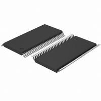
56-TSSOP
Circuit
12 x 1:1
Independent Circuits
2
Current - Output High, Low
15mA, 64mA
Voltage Supply Source
Single Supply
Voltage - Supply
4.5 V ~ 5.5 V
Operating Temperature
-40°C ~ 85°C
Mounting Type
Surface Mount
Propagation Delay Time
0.25 ns at 5 V
Supply Voltage (max)
5.5 V
Supply Voltage (min)
4.5 V
Maximum Operating Temperature
+ 85 C
Minimum Operating Temperature
- 40 C
Logic Family
CBT
Mounting Style
SMD/SMT
On Resistance (max)
14 Ohms
Number Of Bits
24
Number Of Elements
2
Technology
CMOS
Low Level Output Current
128mA
On Resistance
14Ohm
Package Type
TSSOP
Operating Temp Range
-40C to 85C
Operating Temperature Classification
Industrial
Operating Supply Voltage (min)
4.5V
Operating Supply Voltage (typ)
5V
Operating Supply Voltage (max)
5.5V
Quiescent Current
3uA
Pin Count
56
Mounting
Surface Mount
Lead Free Status / RoHS Status
Lead free / RoHS Compliant
Lead Free Status / RoHS Status
Lead free / RoHS Compliant, Lead free / RoHS Compliant
Other names
935269707112
CBT16211DGG
CBT16211DGG
CBT16211DGG
CBT16211DGG


Philips Semiconductors
FEATURES
QUICK REFERENCE DATA
ORDERING INFORMATION
FUNCTION TABLE
H = High voltage level
L = Low voltage level
Z = High impedance “off ” state
56-Pin Plastic SSOP Type III
56-Pin Plastic TSSOP Type II
2001 Jun 13
5
TTL compatible control input levels
Package options include plastic shrink small outline (SSOP),
thin shrink small outline (TSSOP)
ESD protection exceeds 1000 V CDM per JESD22-C101
Latch-up testing is done to JESDEC Standard JESD78 which
exceeds 100 mA
24-bit bus switch with 12-bit output enables
SYMBOL
1OE
switch connection between two ports
C
t
t
C
PLH
PHL
I
H
H
L
L
OUT
CC
IN
INPUTS
PACKAGES
Propagation delay
An to Yn
Input capacitance
Output capacitance
Total supply current
2OE
H
H
L
L
PARAMETER
1A = 1B
1A = 1B
1A, 1B
Z
Z
OUTPUTS
TEMPERATURE RANGE
2A = 2B
2A = 2B
2A, 2B
–40 to 85 C
–40 to 85 C
Z
Z
C
V
Outputs disabled; V
Outputs disabled; V
I
L
= 0 V or V
= 50 pF; V
2
CC
T
CC
amb
output-enable (OE) inputs. It can be used as two 12-bit bus switches
high, the switch is open, and a high-impedance state exists between
DESCRIPTION
The CBT16211 provides 24 bits of high-speed TTL-compatible bus
switching. The low on-state resistance of the switch allows
connections to be made with minimal propagation delay.
The device is organized as a dual 12-bit bus switch with separate
or as one 24-bit bus switch. When OE is low, the associated 12-bit
bus switch is on, and port A is connected to port B. When OE is
the ports.
The CBT16211 is characterized for operation from –40 to 85 C.
LOGIC SYMBOL
= 5 V
= 25 C; GND = 0 V
CONDITIONS
CC
O
= 0 V or V
= 5.5 V
1A12
2A12
1OE
2OE
1A1
2A1
CC
CBT16211DGG
ORDER CODE
CBT16211DL
14
56
15
28
55
2
TYPICAL
54
42
41
29
SA00510
0.25
4.3
6.9
3.0
1B1
1B12
2B1
2B12
CBT16211
DWG NUMBER
SOT371-1
SOT364-1
853-2259 26502
Product data
UNIT
pF
pF
ns
A
Related parts for CBT16211DGG,112
Image
Part Number
Description
Manufacturer
Datasheet
Request
R

Part Number:
Description:
NXP Semiconductors designed the LPC2420/2460 microcontroller around a 16-bit/32-bitARM7TDMI-S CPU core with real-time debug interfaces that include both JTAG andembedded trace
Manufacturer:
NXP Semiconductors
Datasheet:

Part Number:
Description:
NXP Semiconductors designed the LPC2458 microcontroller around a 16-bit/32-bitARM7TDMI-S CPU core with real-time debug interfaces that include both JTAG andembedded trace
Manufacturer:
NXP Semiconductors
Datasheet:
Part Number:
Description:
NXP Semiconductors designed the LPC2468 microcontroller around a 16-bit/32-bitARM7TDMI-S CPU core with real-time debug interfaces that include both JTAG andembedded trace
Manufacturer:
NXP Semiconductors
Datasheet:
Part Number:
Description:
NXP Semiconductors designed the LPC2470 microcontroller, powered by theARM7TDMI-S core, to be a highly integrated microcontroller for a wide range ofapplications that require advanced communications and high quality graphic displays
Manufacturer:
NXP Semiconductors
Datasheet:
Part Number:
Description:
NXP Semiconductors designed the LPC2478 microcontroller, powered by theARM7TDMI-S core, to be a highly integrated microcontroller for a wide range ofapplications that require advanced communications and high quality graphic displays
Manufacturer:
NXP Semiconductors
Datasheet:
Part Number:
Description:
The Philips Semiconductors XA (eXtended Architecture) family of 16-bit single-chip microcontrollers is powerful enough to easily handle the requirements of high performance embedded applications, yet inexpensive enough to compete in the market for hi
Manufacturer:
NXP Semiconductors
Datasheet:
Part Number:
Description:
The XA-S3 device is a member of Philips Semiconductors? XA(eXtended Architecture) family of high performance 16-bitsingle-chip microcontrollers
Manufacturer:
NXP Semiconductors
Datasheet:

Part Number:
Description:
The NXP BlueStreak LH75401/LH75411 family consists of two low-cost 16/32-bit System-on-Chip (SoC) devices
Manufacturer:
NXP Semiconductors
Datasheet:
Part Number:
Description:
The NXP LPC3130/3131 combine an 180 MHz ARM926EJ-S CPU core, high-speed USB2
Manufacturer:
NXP Semiconductors
Datasheet:
Part Number:
Description:
The NXP LPC3141 combine a 270 MHz ARM926EJ-S CPU core, High-speed USB 2
Manufacturer:
NXP Semiconductors
Part Number:
Description:
The NXP LPC3143 combine a 270 MHz ARM926EJ-S CPU core, High-speed USB 2
Manufacturer:
NXP Semiconductors

Part Number:
Description:
The NXP LPC3152 combines an 180 MHz ARM926EJ-S CPU core, High-speed USB 2
Manufacturer:
NXP Semiconductors
Part Number:
Description:
The NXP LPC3154 combines an 180 MHz ARM926EJ-S CPU core, High-speed USB 2
Manufacturer:
NXP Semiconductors

Part Number:
Description:
Standard level N-channel enhancement mode Field-Effect Transistor (FET) in a plastic package using NXP High-Performance Automotive (HPA) TrenchMOS technology
Manufacturer:
NXP Semiconductors
Datasheet: