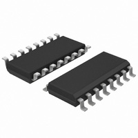
PCA8550D,112 NXP Semiconductors, PCA8550D,112 Datasheet - Page 2

PCA8550D,112
Manufacturer Part Number
PCA8550D,112
Description
IC I2C EEPROM DIP SWITCH 16SOIC
Manufacturer
NXP Semiconductors
Type
Multiplexerr
Datasheet
1.PCA8550PW118.pdf
(12 pages)
Specifications of PCA8550D,112
Circuit
1 x 4:4
Independent Circuits
1
Current - Output High, Low
2mA, 2mA
Voltage Supply Source
Single Supply
Voltage - Supply
3 V ~ 3.6 V
Operating Temperature
0°C ~ 70°C
Mounting Type
Surface Mount
Package / Case
16-SOIC (3.9mm Width)
Operating Temperature (max)
70C
Operating Temperature (min)
0C
Package Type
SO
Pin Count
16
Mounting
Surface Mount
Lead Free Status / RoHS Status
Lead free / RoHS Compliant
Other names
935261457112
PCA8550D
PCA8550D
PCA8550D
PCA8550D
Philips Semiconductors
FEATURES
•
•
•
•
•
•
•
•
•
•
DESCRIPTION
The primary function of the 4-bit 2-to-1 I
either a 4-bit input or data from a non-volatile register and drive this
value onto the output pins. One additional non-multiplexed register
output is also provided. The non-multiplexed output is latched to
prevent output value changes during I
register. A write protect input is provided to enable/disable the ability
to write to the non-volatile register. An “override” input feature forces
all outputs to logic 0.
ORDERING INFORMATION
Standard packing quantities and other packaging data is available at www.philipslogic.com/packaging.
FUNCTIONAL DESCRIPTION
When the MUX_SELECT signal is logic 0, the multiplexer will select
the data from the non-volatile register to drive on the MUX_OUT
pins. When the MUX_SELECT signal is logic 1, the multiplexer will
select the MUX_IN lines to drive on the MUX_OUT pins. The
MUX_SELECT signal is also used to latch the NON_MUXED_OUT
signal which outputs data from the non-volatile register. The
NON_MUXED_OUT signal latch is transparent when MUX_SELECT
is in a logic 0 state, and will latch data when MUX_SELECT is in a
logic 1 state. When the active-LOW OVERRIDE_N signal is set to
logic 0 and the MUX_SELECT signal is at a logic 0, all outputs will
be driven to logic 0. This information is summarized in Table 1.
Pentium II is a registered trademark of Intel Corporation.
2003 Jun 27
4-bit 2-to-1 multiplexer, 1-bit latch DIP switch
5-bit internal non-volatile register
Override input forces all outputs to logic 0
Internal non-volatile register write/readable via I
Write-protect pin enables/disables I
2.5 V multiplexed outputs
3.3 V non-multiplexed output (latched)
5 V tolerant inputs
Useful for ‘jumperless’ configuration of PC motherboards
Designed for use in Pentium Pro/Pentium II systems
4-bit multiplexed/1-bit latched 5-bit
I
16-Pin Plastic TSSOP
16-Pin Plastic SSOP
2
16-Pin Plastic SO
C EEPROM DIP switch
PACKAGES
TEMPERATURE RANGE
0 to +70 °C
0 to +70 °C
0 to +70 °C
2
2
C writes to register
C writes to the non-volatile
2
C multiplexer is to select
2
C-bus
ORDER CODE
PCA8550PW
PCA8550DB
PCA8550D
2
PIN CONFIGURATION
The write protect (WP) input is used to control the ability to write the
contents of the 5-bit non-volatile register. If the WP signal is logic 0,
the I
register. If the WP signal is logic 1, data will not be allowed to be
written into the non-volatile register.
The factory default for the contents of the non-volatile register are all
logic 0. These stored values can be read or written using the
I
The OVERRIDE_N, WP, MUX_IN, and MUX_SELECT signals have
internal pull-up resistors. See the DC and AC Characteristics for
hysteresis and signal spike suppression figures.
2
C bus (described in the next section).
2
C-bus will be able to write the contents of the non-volatile
OVERRIDE_N
MUX_IN A
MUX_IN B
MUX_IN C
MUX_IN D
TOPSIDE MARK
I
I
2
2
C SDA
C SCL
GND
Figure 1. Pin configuration
PCA8550
PCA8550
PA8550
1
2
3
4
5
6
7
8
16
15
14
13
12
11
10
9
V
WP
NON_MUXED_OUT
MUX_SELECT
MUX_OUT A
MUX_OUT B
MUX_OUT C
MUX_OUT D
DRAWING NUMBER
CC
SW00579
SOT109-1
SOT338-1
SOT403-1
PCA8550
Product data


