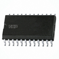
CBTD3384D,118 NXP Semiconductors, CBTD3384D,118 Datasheet - Page 4

CBTD3384D,118
Manufacturer Part Number
CBTD3384D,118
Description
IC BUS SWITCH 10BIT 24-SOIC
Manufacturer
NXP Semiconductors
Series
74CBTDr
Type
Bus Switchr
Datasheet
1.CBTD3384D112.pdf
(17 pages)
Specifications of CBTD3384D,118
Circuit
5 x 1:1
Independent Circuits
2
Current - Output High, Low
15mA, 64mA
Voltage Supply Source
Single Supply
Voltage - Supply
4.5 V ~ 5.5 V
Operating Temperature
-40°C ~ 85°C
Mounting Type
Surface Mount
Package / Case
24-SOIC (7.5mm Width)
Lead Free Status / RoHS Status
Lead free / RoHS Compliant
Other names
935269654118
CBTD3384D-T
CBTD3384D-T
CBTD3384D-T
CBTD3384D-T
NXP Semiconductors
7. Limiting values
Table 4.
In accordance with the Absolute Maximum Rating System (IEC 60134).
T
[1]
[2]
8. Recommended operating conditions
Table 5.
All unused control inputs of the device must be held at V
9. Static characteristics
Table 6.
Voltages are referenced to GND (ground = 0 V).
CBTD3384
Product data sheet
Symbol
V
V
I
I
T
Symbol
V
V
V
T
Symbol
V
I
I
ΔI
V
C
C
O
IK
I
CC
amb
stg
amb
CC
I
CC
IH
IL
IK
pass
I
io(off)
CC
Stresses beyond those listed may cause permanent damage to the device. These are stress ratings only and functional operation of the
device at these or any other conditions beyond those indicated under
conditions for extended periods may affect device reliability.
The input and output negative-voltage ratings may be exceeded if the input and output clamp-current ratings are observed.
=
−
40
°
Parameter
input clamping voltage
input leakage current
supply current
additional supply current
pass voltage
input capacitance
off-state input/output
capacitance
Limiting values
Operating conditions
Static characteristics
C to +85
Parameter
supply voltage
HIGH-level input voltage
LOW-level input voltage
ambient temperature
Parameter
supply voltage
input voltage
output current
input clamping current
storage temperature
°
C, unless otherwise specified.
Conditions
V
V
V
V
per input pin; V
at 3.4 V, other inputs at V
see
control pins; V
port off; V
CC
CC
CC
I
= V
All information provided in this document is subject to legal disclaimers.
Figure 5
= 4.5 V; I
= 5.5 V; V
= 5.5 V; I
CC
or GND
Rev. 5 — 19 November 2010
operating in free air
I
Conditions
= 3 V or 0 V; nOE = V
to
I
O
I
I
= −18 mA
CC
= 3 V or 0 V
= GND or 5.5 V
= 0 mA;
Figure 9
Conditions
V
V
CC
10-bit level shifting bus switch with 5-bit output enables
O
I/O
= 5.5 V; one input
or GND to ensure proper device operation.
< 0 V
= 0 V
CC
Section 8.
or GND
[1]
CC
is not implied. Exposure to absolute-maximum-rated
[2]
Min
4.5
2.0
-
−40
Min
[2]
T
-
-
-
-
-
-
-
amb
Min
−0.5
−0.5
-
−50
−65
= −40 °C to +85 °C
Typ
-
-
-
-
Typ
3.2
6.0
-
-
-
-
-
CBTD3384
[1]
Max
+7.0
+7.0
±128
-
+150
© NXP B.V. 2010. All rights reserved.
Max
5.5
-
0.8
+85
Max
−1.2
1.5
2.5
±1
-
-
-
Unit
V
V
mA
mA
°C
Unit
V
V
V
°C
pF
Unit
V
μA
mA
mA
V
pF
4 of 17


