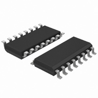
N74F138D,602 NXP Semiconductors, N74F138D,602 Datasheet - Page 2

N74F138D,602
Manufacturer Part Number
N74F138D,602
Description
IC DECODER/DEMUX 3-8LINE 16SOIC
Manufacturer
NXP Semiconductors
Series
74Fr
Type
Decoder/Demultiplexerr
Datasheet
1.N74F138D602.pdf
(8 pages)
Specifications of N74F138D,602
Circuit
1 x 3:8
Independent Circuits
1
Current - Output High, Low
1mA, 20mA
Voltage Supply Source
Single Supply
Voltage - Supply
4.5 V ~ 5.5 V
Operating Temperature
0°C ~ 70°C
Mounting Type
Surface Mount
Package / Case
16-SOIC (3.9mm Width)
Lead Free Status / RoHS Status
Lead free / RoHS Compliant
Other names
933739450602
N74F138D
N74F138D
N74F138D
N74F138D
One (1.0) FAST unit load is defined as: 20 A in the High state and 0.6mA in the Low state.
Philips Semiconductors
FEATURE
DESCRIPTION
The 74F138 decoder accepts three binary weighted inputs (A0, A1,
A2) and when enabled, provides eight mutually exclusive, active low
outputs (Q0 – Q7). The device features three enable inputs; two
active low (E0, E1) and one active high (E2). Every output will be
high unless E0 and E1 are low and E2 is high. This multiple enable
function allows easy parallel expansion of the device to 1-of-32
(5 lines to 32 lines) decoder with just four 74F138s and one inverter
(see Figure 1). The device can be used as an eight output
demultiplexer by using one of the active low enable inputs as the
data input and the remaining enable inputs as strobes. Enable
inputs not used must be permanently tied to their appropriate active
high or active low state.
ORDERING INFORMATION
INPUT AND OUTPUT LOADING AND FAN-OUT TABLE
NOTE:
LOGIC SYMBOL
February 14, 1991
Multiple input enable for easy expansion
Ideal for memory chip select decoding
Industrial temperature range available (–40 C to +85 C)
V
GND = Pin 8
1-of-8 decoder/demultiplexer
Demultiplexing capability
16-pin plastic DIP
16-pin plastic SO
CC
DESCRIPTION
= Pin 16
Q0 – Q7
A0 – A2
E0, E1
4
5
6
PINS
E2
E0
E1
E2
Q0
15
V
Q1
Address inputs
Enable inputs (active Low)
Enable input (active High)
Data outputs
14
CC
Q2 Q3 Q4 Q5
13 12 11 10
= 5V 10%, T
1
A0
COMMERCIAL RANGE
A1 A2
2
3
N74F138N
N74F138D
DESCRIPTION
Q6
amb
SF00175
9
Q7
7
= 0 C to +70 C
ORDER CODE
2
V
PIN CONFIGURATION
IEC/IEEE SYMBOL
CC
74F138
TYPE
= 5V 10%, T
74F (U.L.) HIGH/LOW
INDUSTRIAL RANGE
1.0/1.0
1.0/1.0
1.0/1.0
50/33
I74F138N
I74F138D
1
2
3
4
5
6
PROPAGATION
amb
GND
TYPICAL
Q7
A0
A1
A2
E0
E1
E2
DELAY
= –40 C to +85 C
5.8ns
1
2
3
4
5
6
7
8
0
2
&
DMUX
G
0
3
LOAD VALUE HIGH/LOW
SF00174
0
1
2
3
4
5
6
7
16
15
14
13
12
10
11
9
SUPPLY CURRENT
1.0mA/20mA
20 A/0.6mA
20 A/0.6mA
20 A/0.6mA
V
Q0
Q1
Q2
Q3
Q4
Q5
Q6
Product specification
SF00176
CC
TYPICAL
(TOTAL)
PKG DWG #
853–0343 01719
13mA
15
14
13
12
11
10
9
7
SOT109-1
SOT38-4
74F138


