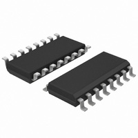
HEF4028BT,653 NXP Semiconductors, HEF4028BT,653 Datasheet - Page 6

HEF4028BT,653
Manufacturer Part Number
HEF4028BT,653
Description
IC 1 OF 10 DECODER 16SOIC
Manufacturer
NXP Semiconductors
Series
4000Br
Type
Decoderr
Specifications of HEF4028BT,653
Package / Case
16-SOIC (3.9mm Width)
Circuit
1 x 4:10
Independent Circuits
1
Voltage Supply Source
Dual Supply
Voltage - Supply
4.5 V ~ 15.5 V
Mounting Type
Surface Mount
Logic Family
HEF4000
Number Of Lines (input / Output)
4.0 / 10.0
Propagation Delay Time
50 ns
Supply Voltage (max)
15 V
Supply Voltage (min)
3 V
Maximum Operating Temperature
+ 85 C
Minimum Operating Temperature
- 40 C
Mounting Style
SMD/SMT
Number Of Input Lines
4.0
Number Of Output Lines
10.0
Logical Function
Decoder/Demux
Number Of Elements
1
Polarity
Non-Inverting
Number Of Inputs
4
Number Of Outputs
10
Output Type
Standard
Package Type
SOIC W
High Level Output Current
-3.6mA
Low Level Output Current
3.6mA
Operating Supply Voltage (typ)
3.3/5/9/12V
Operating Supply Voltage (max)
15V
Operating Supply Voltage (min)
3V
Operating Temp Range
-40C to 85C
Operating Temperature Classification
Industrial
Mounting
Surface Mount
Pin Count
16
Quiescent Current
80uA
Technology
CMOS
Lead Free Status / RoHS Status
Lead free / RoHS Compliant
Operating Temperature
-
Current - Output High, Low
-
Lead Free Status / Rohs Status
Lead free / RoHS Compliant
Other names
933372800653
HEF4028BTD-T
HEF4028BTD-T
HEF4028BTD-T
HEF4028BTD-T
NXP Semiconductors
Table 7.
V
[1]
Table 8.
P
12. Waveforms
Table 9.
HEF4028B_6
Product data sheet
Symbol Parameter
t
Symbol
P
Supply voltage
V
5 V to 15 V
t
SS
D
Fig 4.
D
DD
can be calculated from the formulas shown. V
= 0 V; T
The typical values of the propagation delay and transition times are calculated from the extrapolation formulas shown (C
transition time
Output shown going high when address input goes low, see
Measurement points are given in
Logic levels: V
Input rise and fall times, propagation delays and output transition times
Dynamic characteristics
Dynamic power dissipation P
Parameter
dynamic power
dissipation
Measurement points
amb
= 25
Yn output
An input
°
C.
OL
and V
V
V
V
OH
SS
OL
V
I
OH
V
10 V
15 V
Conditions
see
5 V
DD
are typical output voltage levels that occur with the output load.
90 %
Figure 4
…continued
V
Table
M
Input
V
0.5V
V
Typical formula for P
P
P
P
10 %
D
M
M
t
PHL
D
D
D
t
THL
9.
= 350 × f
= 2200 × f
= 7350 × f
DD
Rev. 06 — 25 November 2009
SS
= 0 V; t
V
10 V
15 V
5 V
DD
i
+ Σ(f
i
i
+ Σ(f
+ Σ(f
r
= t
o
[1]
t
o
o
× C
PLH
f
t
× C
× C
TLH
≤
Table
Extrapolation formula
10 ns + (1.00 ns/pF)C
D
9 ns + (0.42 ns/pF)C
6 ns + (0.28 ns/pF)C
20 ns; T
L
) × V
(μW)
L
L
) × V
) × V
3.
DD
DD
DD
amb
2
2
2
= 25
°
V
0.5V
C.
Output
M
where:
f
f
C
V
Σ(f
i
o
L
L
L
DD
= input frequency in MHz;
L
= output frequency in MHz;
o
DD
= output load capacitance in pF;
× C
= supply voltage in V;
L
t
t
) = sum of the outputs.
Min
-
-
-
BCD to decimal decoder
001aah859
HEF4028B
Typ
60
30
20
© NXP B.V. 2009. All rights reserved.
Max
120
L
60
40
in pF).
Unit
ns
ns
ns
6 of 12


