CBT3125PW,118 NXP Semiconductors, CBT3125PW,118 Datasheet - Page 4
CBT3125PW,118
Manufacturer Part Number
CBT3125PW,118
Description
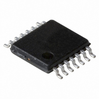
IC FET BUS SWITCH QUAD 14TSSOP
Manufacturer
NXP Semiconductors
Series
74CBTr
Type
FET Bus Switchr
Datasheet
1.CBT3125DB118.pdf
(10 pages)
Specifications of CBT3125PW,118
Package / Case
14-TSSOP
Circuit
1 x 1:1
Independent Circuits
4
Current - Output High, Low
15mA, 64mA
Voltage Supply Source
Single Supply
Voltage - Supply
4.5 V ~ 5.5 V
Operating Temperature
-40°C ~ 85°C
Mounting Type
Surface Mount
Number Of Switches
Quad
Propagation Delay Time
0.25 ns
Supply Voltage (max)
5.5 V
Supply Voltage (min)
4.5 V
Maximum Operating Temperature
+ 85 C
Minimum Operating Temperature
- 40 C
Logic Family
CBT
Mounting Style
SMD/SMT
On Resistance (max)
15 Ohms
Lead Free Status / RoHS Status
Lead free / RoHS Compliant
Lead Free Status / RoHS Status
Lead free / RoHS Compliant, Lead free / RoHS Compliant
Other names
935270670118
CBT3125PWDH-T
CBT3125PWDH-T
CBT3125PWDH-T
CBT3125PWDH-T


1. All typical values are at V
2. This is the increase in supply current for each input that is at the specified TTL voltage level rather than V
3. Measured by the voltage drop between the A and the B terminals at the indicated current through the switch. On-state resistance is
1. This parameter is warranted but not production tested. The propagation delay is based on the RC time constant of the typical on-state
Philips Semiconductors
DC ELECTRICAL CHARACTERISTICS
Over recommended operating free-air temperature range, unless otherwise noted.
NOTES:
AC CHARACTERISTICS
T
NOTE:
2001 Dec 12
amb
SYMBOL
C
Quadruple FET bus switch
SYMBOL
SYMBOL
determined by the lower of the voltages of the two (A or B) terminals.
resistance of the switch and a load capacitance of 50 pF, when driven by an ideal voltage source (zero output impedance).
IO(OFF)
V
I
V
r
= –40 to +85 C; C
C
CC
I
I
on
CC
IK
t
t
t
I
P
I
dis
pd
en
Input clamp voltage
Input leakage current
Quiescent supply current
Additional supply current per
input pin (Note 2)
Input capacitance
Power-off leakage current
Pass gate voltage
On-resistance (Note 3)
Propagation delay
Output enable time
to High and Low level
Output disable time
from High and Low level
L
= 50 pF, unless otherwise noted.
CC
PARAMETER
PARAMETER
PARAMETER
= 5 V, unless otherwise noted. T
1
control inputs
control inputs
V
I
V
V
V
V
V
one input at 3.4 V,
other inputs at V
V
V
V
V
I
V
I
V
I
amb
I
I
I
I
CC
CC
I
CC
I
CC
I
O
CC
CC
CC
CC
(INPUT)
= –18 mA
= 64 mA
= 30 mA
= –15 mA
FROM
= 5.5 V or GND
= V
= 3 V or 0
A or B
= 3 V or 0; OE = V
OE
OE
= 25 C.
= 4.5 V;
= 5.5 V;
= 5.5 V; I
= 5.5 V;
= 5.0 V; V
= 4.5 V; V
= 4.5 V; V
= 4.5 V; V
CC
CONDITIONS
4
or GND
O
I
I
I
I
= 0;
= 5.0 V
= 0 V;
= 0 V;
= 2.4 V;
CC
or GND
(OUTPUT)
CC
B or A
A or B
A or B
TO
MIN.
—
—
—
—
—
—
—
—
—
—
Min
1.0
—
V
1
CC
CC
TYP.
= 5 V
or GND.
1.7
3.4
3.8
—
—
—
—
10
5
5
1
0.5 V
Max
0.25
5.4
4.7
MAX.
CBT3125
–1.2
2.5
15
—
—
—
3
7
7
1
Product data
UNIT
UNIT
ns
ns
ns
UNIT
mA
pF
pF
V
V
A
A
Related parts for CBT3125PW,118
Image
Part Number
Description
Manufacturer
Datasheet
Request
R

Part Number:
Description:
Manufacturer:
NXP Semiconductors
Datasheet:
Part Number:
Description:
Cbt3125 Quadruple Fet Bus Switch
Manufacturer:
NXP Semiconductors
Datasheet:
Part Number:
Description:
NXP Semiconductors designed the LPC2420/2460 microcontroller around a 16-bit/32-bitARM7TDMI-S CPU core with real-time debug interfaces that include both JTAG andembedded trace
Manufacturer:
NXP Semiconductors
Datasheet:

Part Number:
Description:
NXP Semiconductors designed the LPC2458 microcontroller around a 16-bit/32-bitARM7TDMI-S CPU core with real-time debug interfaces that include both JTAG andembedded trace
Manufacturer:
NXP Semiconductors
Datasheet:
Part Number:
Description:
NXP Semiconductors designed the LPC2468 microcontroller around a 16-bit/32-bitARM7TDMI-S CPU core with real-time debug interfaces that include both JTAG andembedded trace
Manufacturer:
NXP Semiconductors
Datasheet:
Part Number:
Description:
NXP Semiconductors designed the LPC2470 microcontroller, powered by theARM7TDMI-S core, to be a highly integrated microcontroller for a wide range ofapplications that require advanced communications and high quality graphic displays
Manufacturer:
NXP Semiconductors
Datasheet:
Part Number:
Description:
NXP Semiconductors designed the LPC2478 microcontroller, powered by theARM7TDMI-S core, to be a highly integrated microcontroller for a wide range ofapplications that require advanced communications and high quality graphic displays
Manufacturer:
NXP Semiconductors
Datasheet:
Part Number:
Description:
The Philips Semiconductors XA (eXtended Architecture) family of 16-bit single-chip microcontrollers is powerful enough to easily handle the requirements of high performance embedded applications, yet inexpensive enough to compete in the market for hi
Manufacturer:
NXP Semiconductors
Datasheet:
Part Number:
Description:
The XA-S3 device is a member of Philips Semiconductors? XA(eXtended Architecture) family of high performance 16-bitsingle-chip microcontrollers
Manufacturer:
NXP Semiconductors
Datasheet:

Part Number:
Description:
The NXP BlueStreak LH75401/LH75411 family consists of two low-cost 16/32-bit System-on-Chip (SoC) devices
Manufacturer:
NXP Semiconductors
Datasheet:
Part Number:
Description:
The NXP LPC3130/3131 combine an 180 MHz ARM926EJ-S CPU core, high-speed USB2
Manufacturer:
NXP Semiconductors
Datasheet:
Part Number:
Description:
The NXP LPC3141 combine a 270 MHz ARM926EJ-S CPU core, High-speed USB 2
Manufacturer:
NXP Semiconductors
Part Number:
Description:
The NXP LPC3143 combine a 270 MHz ARM926EJ-S CPU core, High-speed USB 2
Manufacturer:
NXP Semiconductors

Part Number:
Description:
The NXP LPC3152 combines an 180 MHz ARM926EJ-S CPU core, High-speed USB 2
Manufacturer:
NXP Semiconductors