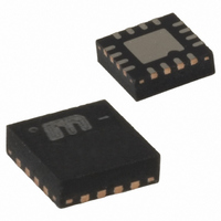
SY89840UMG Micrel Inc, SY89840UMG Datasheet - Page 8

SY89840UMG
Manufacturer Part Number
SY89840UMG
Description
IC MUX 2:1 LVPECL DIFF 16MLF
Manufacturer
Micrel Inc
Series
SY89r
Type
Multiplexerr
Datasheet
1.SY89840UMG.pdf
(15 pages)
Specifications of SY89840UMG
Circuit
1 x 2:1
Independent Circuits
1
Voltage Supply Source
Single Supply
Voltage - Supply
3 V ~ 3.6 V
Operating Temperature
-40°C ~ 85°C
Mounting Type
Surface Mount
Package / Case
16-MLF®, QFN
Number Of Clock Inputs
2
Mode Of Operation
Differential
Output Logic Level
LVPECL
Operating Supply Voltage (min)
2.375V
Operating Supply Voltage (typ)
2.5/3.3V
Operating Supply Voltage (max)
3.6V
Package Type
MLF
Operating Temp Range
-40C to 85C
Operating Temperature Classification
Industrial
Signal Type
CML/LVDS/PECL
Mounting
Surface Mount
Pin Count
16
Lead Free Status / RoHS Status
Lead free / RoHS Compliant
Current - Output High, Low
-
Lead Free Status / Rohs Status
Compliant
Other names
576-1434
Available stocks
Company
Part Number
Manufacturer
Quantity
Price
Company:
Part Number:
SY89840UMG
Manufacturer:
MICREL
Quantity:
33
February 2005
Functional Description
RPE MUX and Fail-Safe Input
The SY89840U is optimized for clock switchover
applications where switching from one clock to
another clock without runt pulses (short cycles) is
required. It features two unique circuits:
Runt-Pulse Eliminator (RPE) Circuit:
The RPE MUX provides a “glitchless” switchover
between two clocks and prevents any runt pulses
from occurring during the switchover transition. The
design of both clock inputs is identical (i.e., the
switchover sequence and protection is symmetrical
for both input pair, IN0 or IN1. Thus, either input pair
may be defined as the primary input). If not required,
the RPE function can be permanently disabled to
allow the switchover between inputs to occur
immediately. If the CAP pin is tied directly to V
the RPE function will be disabled and the multiplexer
will function as a normal multiplexer.
Fail-Safe Input (FSI) Circuit:
The FSI function provides protection against a
selected input pair that drops below the minimum
amplitude requirement. If the selected input pair
drops sufficiently below the 100mV minimum single-
ended input amplitude limit (V
differentially (V
valid clock state.
DIFF_IN
), the output will latch to the last
IN
), or 200mV
Timing Diagram 1
CC
,
8
RPE and FSI Functionality
The basic operation of the RPE MUX and FSI
functionality is described with the following four case
descriptions. All descriptions are related to the true
inputs and outputs. The primary (or selected) clock
is called CLK1; the secondary (or alternate) clock is
called CLK2. Due to the totally asynchronous
relation of the IN and SEL signals and an additional
internal protection against metastability, the number
of pulses required for the operations described in
cases 1-4 can vary within certain limits. Refer to
“Timing Diagrams” for more detailed information.
Case #1 Two Normal Clocks and RPE Enabled
In this case the frequency difference between the
two running clocks IN0 and IN1 must not be greater
than 1.5:1. For example, if the IN0 clock is 500MHz,
the IN1 clock must be within the range of 334MHz to
750MHz.
If the SEL input changes state to select the alternate
clock, the switchover from CLK1 to CLK2 will occur
in three stages.
•
•
•
Stage 1: The output will continue to follow CLK1 for
a limited number of pulses.
Stage 2: The output will remain LOW for a limited
number of pulses of CLK2.
Stage 3: The output follows CLK2.
hbwhelp@micrel.com
or (408) 955-1690
M9999-021705


