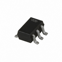
74AUP1G157GW,125 NXP Semiconductors, 74AUP1G157GW,125 Datasheet - Page 10

74AUP1G157GW,125
Manufacturer Part Number
74AUP1G157GW,125
Description
IC MUX LP 2-INPUT SC-88
Manufacturer
NXP Semiconductors
Series
74AUPr
Type
Multiplexerr
Datasheet
1.74AUP1G157GM115.pdf
(20 pages)
Specifications of 74AUP1G157GW,125
Package / Case
SC-70-6, SC-88, SOT-363
Circuit
1 x 2:1
Independent Circuits
1
Current - Output High, Low
4mA, 4mA
Voltage Supply Source
Single Supply
Voltage - Supply
0.8 V ~ 3.6 V
Operating Temperature
-40°C ~ 125°C
Mounting Type
Surface Mount
Product
Multiplexer
Logic Family
AUP
Number Of Lines (input / Output)
2.0 / 1.0
Propagation Delay Time
19.1 ns at 1.1 V to 1.3 V, 11.1 ns at 1.4 V to 1.6 V, 8.9 ns at 1.65 V to 1.95 V
Supply Voltage (max)
3.6 V
Supply Voltage (min)
0.8 V
Maximum Operating Temperature
+ 125 C
Minimum Operating Temperature
- 40 C
Mounting Style
SMD/SMT
Number Of Input Lines
2.0
Number Of Output Lines
1.0
Logical Function
Mux
Configuration
1 x 2:1
Number Of Inputs
2
Number Of Outputs
1
Operating Supply Voltage (typ)
1.8/2.5/3.3V
Operating Supply Voltage (min)
0.8V
Operating Supply Voltage (max)
3.6V
Power Dissipation
250mW
Operating Temp Range
-40C to 125C
Operating Temperature Classification
Automotive
Mounting
Surface Mount
Pin Count
6
Package Type
SC-88
Lead Free Status / RoHS Status
Lead free / RoHS Compliant
Lead Free Status / RoHS Status
Lead free / RoHS Compliant, Lead free / RoHS Compliant
Other names
568-4986-2
74AUP1G157GW,125
74AUP1G157GW-G
74AUP1G157GW-G
935279969125
74AUP1G157GW,125
74AUP1G157GW-G
74AUP1G157GW-G
935279969125
NXP Semiconductors
Table 8.
Voltages are referenced to GND (ground = 0 V); for test circuit see
[1]
[2]
[3]
12. Waveforms
Table 9.
74AUP1G157
Product data sheet
Symbol Parameter
C
C
Supply voltage
V
0.8 V to 3.6 V
Fig 8.
CC
L
PD
= 5 pF, 10 pF, 15 pF and 30 pF
All typical values are measured at nominal V
t
C
P
f
f
C
V
N = number of inputs switching;
Σ(C
pd
i
o
D
CC
PD
= input frequency in MHz;
L
= output frequency in MHz;
is the same as t
= output load capacitance in pF;
= C
L
is used to determine the dynamic power dissipation (P
= supply voltage in V;
× V
power dissipation
capacitance
Measurement points are given in
Logic levels: V
The data inputs (I0, I1) and common data select input (S) to output (Y) propagation delays
PD
Dynamic characteristics
Measurement points
CC
× V
2
× f
CC
o
2
) = sum of the outputs.
× f
PLH
i
× N + Σ(C
OL
I0, I1, S input
Y output
and t
and V
PHL
Output
V
0.5 × V
Conditions
f
i
OH
L
M
= 1 MHz; V
.
V
V
V
V
V
V
× V
GND
V
V
are typical output voltage drop that occur with the output load.
CC
CC
CC
CC
CC
CC
OH
OL
V
CC
I
= 0.8 V
= 1.1 V to 1.3 V
= 1.4 V to 1.6 V
= 1.65 V to 1.95 V
= 2.3 V to 2.7 V
= 3.0 V to 3.6 V
CC
2
…continued
× f
Table
o
All information provided in this document is subject to legal disclaimers.
) where:
I
CC
= GND to V
9.
.
Rev. 3 — 28 October 2010
V
M
Input
V
0.5 × V
M
CC
V
D
t
M
PHL
in μW).
CC
[3]
Figure
Min
-
-
-
-
-
-
Typ
9.
25 °C
2.6
2.7
2.8
2.9
3.4
4.0
[1]
V
V
I
CC
Max
-
-
-
-
-
-
Low-power 2-input multiplexer
t
PLH
Min
-
-
-
-
-
-
74AUP1G157
001aac658
−40 °C to +125 °C
(85 °C)
Max
t
≤ 3.0 ns
r
-
-
-
-
-
-
= t
© NXP B.V. 2010. All rights reserved.
f
(125 °C)
Max
-
-
-
-
-
-
10 of 20
Unit
pF
pF
pF
pF
pF
pF


