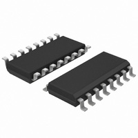
74HCT670D,653 NXP Semiconductors, 74HCT670D,653 Datasheet - Page 8

74HCT670D,653
Manufacturer Part Number
74HCT670D,653
Description
IC 4X4 REGISTER FILE 3ST 16SOIC
Manufacturer
NXP Semiconductors
Series
74HCTr
Datasheet
1.74HCT670DB112.pdf
(9 pages)
Specifications of 74HCT670D,653
Logic Type
Register, Bidirectional
Package / Case
16-SOIC (3.9mm Width)
Output Type
Standard
Number Of Elements
1
Number Of Bits Per Element
4
Function
Universal
Voltage - Supply
4.5 V ~ 5.5 V
Operating Temperature
-40°C ~ 125°C
Mounting Type
Surface Mount
Logic Family
HCT
Number Of Circuits
1
Propagation Delay Time
50 ns
High Level Output Current
- 6 mA
Low Level Output Current
6 mA
Supply Voltage (max)
5.5 V
Maximum Operating Temperature
+ 125 C
Minimum Operating Temperature
- 40 C
Mounting Style
SMD/SMT
Supply Voltage (min)
4.5 V
Logical Function
Register File
Number Of Elements
1
Number Of Bits
4
Number Of Inputs
4
Number Of Outputs
4
Operating Supply Voltage (typ)
5V
Operating Supply Voltage (max)
5.5V
Operating Supply Voltage (min)
4.5V
Polarity
Non-Inverting
Technology
CMOS
Mounting
Surface Mount
Pin Count
16
Operating Temp Range
-40C to 125C
Operating Temperature Classification
Automotive
Quiescent Current
8uA
Lead Free Status / RoHS Status
Lead free / RoHS Compliant
Lead Free Status / RoHS Status
Lead free / RoHS Compliant, Lead free / RoHS Compliant
Other names
74HCT670D-T
74HCT670D-T
933715410653
74HCT670D-T
933715410653
Philips Semiconductors
AC WAVEFORMS
December 1990
4 x 4 register file; 3-state
(1) HC : V
Fig.6
(1) HC : V
The shaded areas indicate when the input is permitted
to change for predictable output performance.
The time allowed for the internal output of the latch to
assume the state of the new data (t
only when attempting to read from a location
immediately after that location has received new data.
This parameter is measured from the falling edge of
WE to the rising edge of R
Fig.8
HCT : V
HCT : V
Waveforms showing the read address input
(R
and output transition times.
Waveforms showing the write address input (W
hold and latch times.
M
M
M
M
A
= 50%; V
= 1.3 V; V
= 50%; V
= 1.3 V; V
, R
B
) to output (Q
I
I
I
I
= GND to V
= GND to V
= GND to 3 V.
= GND to 3 V.
A
or R
B
, RE must be LOW.
latch
CC
CC
n
.
.
) is important
) propagation delays
A
8
, W
B
) and data input (D
(1) HC : V
Fig.7
HCT : V
Waveforms showing the write enable input
(WE) and data input (D
propagation delays, and the write enable
pulse width.
M
M
= 50%; V
= 1.3 V; V
I
n
I
= GND to V
) to write enable (WE) set-up,
= GND to 3 V.
CC
.
74HC/HCT670
n
) to output (Q
Product specification
n
)


