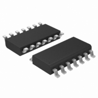
MC74HCT14ADG ON Semiconductor, MC74HCT14ADG Datasheet

MC74HCT14ADG
Specifications of MC74HCT14ADG
MC74HCT14ADGOS
Related parts for MC74HCT14ADG
MC74HCT14ADG Summary of contents
Page 1
MC74HCT14A Hex Schmitt−Trigger Inverter with LSTTL Compatible Inputs High−Performance Silicon−Gate CMOS The MC74HCT14A may be used as a level converter for interfacing TTL or NMOS outputs to high−speed CMOS inputs. The HCT14A is useful to “square up” slow input rise ...
Page 2
... ORDERING INFORMATION Device MC74HCT14AN MC74HCT14ANG MC74HCT14AD MC74HCT14ADG MC74HCT14ADR2 MC74HCT14ADR2G MC74HCT14ADTR2 MC74HCT14ADTR2G MC74HCT14AFEL MC74HCT14AFELG †For information on tape and reel specifications, including part orientation and tape sizes, please refer to our Tape and Reel Packaging Specifications Brochure, BRD8011/D. *This package is inherently Pb−Free. LOGIC DIAGRAM ...
Page 3
... Tested to EIA/JESD22−A114−A. 2. Tested to EIA/JESD22−A115−A. 3. Tested to JESD22−C101−A. 4. Tested to EIA/JESD78. 5. For high frequency or heavy load considerations, see the ON Semiconductor High−Speed CMOS Data Book (DL129/D). RECOMMENDED OPERATING CONDITIONS Symbol Î Î Î Î Î Î Î Î Î Î Î Î Î Î Î Î Î Î Î Î Î Î Î Î Î ...
Page 4
... Output Î Î Î Î Î Î Î Î Î Î Î Î 9. For propagation delays with loads other than 50 pF, and information on typical parametric values, see the ON Semiconductor High−Speed CMOS Data Book (DL129/D). C Power Dissipation Capacitance, per Inverter (Note 10) PD 10. Used to determine the no− ...
Page 5
INPUT A 2.7 V 1 PLH 90% 1.3 V OUTPUT Y 10 TLH THL Figure 1. Switching Waveforms TEST POINT OUTPUT DEVICE UNDER TEST *Includes all probe and jig capacitance. Figure 2. ...
Page 6
−T− SEATING PLANE 0.13 (0.005) PACKAGE DIMENSIONS PDIP−14 CASE 646−06 ISSUE http://onsemi.com 6 NOTES: 1. DIMENSIONING AND TOLERANCING PER ANSI ...
Page 7
... G −T− SEATING 14 PL PLANE 0.25 (0.010 14X 0.58 *For additional information on our Pb−Free strategy and soldering details, please download the ON Semiconductor Soldering and Mounting Techniques Reference Manual, SOLDERRM/D. PACKAGE DIMENSIONS SOIC−14 CASE 751A−03 ISSUE 0.25 (0.010 ...
Page 8
... S A −V− C 0.10 (0.004) −T− SEATING G D PLANE 14X 0.36 *For additional information on our Pb−Free strategy and soldering details, please download the ON Semiconductor Soldering and Mounting Techniques Reference Manual, SOLDERRM/D. PACKAGE DIMENSIONS TSSOP−14 CASE 948G−01 ISSUE 0.25 (0.010) ...
Page 9
... Opportunity/Affirmative Action Employer. This literature is subject to all applicable copyright laws and is not for resale in any manner. PUBLICATION ORDERING INFORMATION LITERATURE FULFILLMENT: Literature Distribution Center for ON Semiconductor P.O. Box 5163, Denver, Colorado 80217 USA Phone: 303−675−2175 or 800−344−3860 Toll Free USA/Canada Fax: 303− ...


