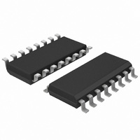
74HC4094D,653 NXP Semiconductors, 74HC4094D,653 Datasheet - Page 12

74HC4094D,653
Manufacturer Part Number
74HC4094D,653
Description
IC REGISTER BUS 8STAGE 16SOIC
Manufacturer
NXP Semiconductors
Series
74HCr
Type
Not Requiredr
Specifications of 74HC4094D,653
Package / Case
16-SOIC (3.9mm Width)
Logic Type
Shift Register
Output Type
Standard
Function
Serial to Parallel
Number Of Elements
1
Number Of Bits Per Element
8
Voltage - Supply
2 V ~ 6 V
Operating Temperature
-40°C ~ 125°C
Mounting Type
Surface Mount
Counting Sequence
Serial to Serial/Parallel
Number Of Circuits
1
Logic Family
HC
Propagation Delay Time
195 ns, 39 ns, 33 ns
Supply Voltage (max)
6 V
Maximum Operating Temperature
+ 125 C
Minimum Operating Temperature
- 40 C
Mounting Style
SMD/SMT
Technology
CMOS
Number Of Elements
1
Number Of Bits
8
Logical Function
Shift Register
Operating Supply Voltage (typ)
5V
Package Type
SO
Operating Temp Range
-40C to 125C
Operating Supply Voltage (min)
2V
Operating Supply Voltage (max)
6V
Operating Temperature Classification
Automotive
Mounting
Surface Mount
Pin Count
16
Lead Free Status / RoHS Status
Lead free / RoHS Compliant
Lead Free Status / RoHS Status
Lead free / RoHS Compliant, Lead free / RoHS Compliant
Other names
568-2265-2
74HC4094D-T
933714850653
74HC4094D-T
933714850653
NXP Semiconductors
[3]
[4]
[5]
12. Waveforms
74HC_HCT4094
Product data sheet
Fig 8.
t
t
C
P
f
f
C
V
N = number of inputs switching;
∑(C
dis
t
i
o
D
CC
PD
= input frequency in MHz;
L
is the same as t
= output frequency in MHz;
= output load capacitance in pF;
= C
is the same as t
L
is used to determine the dynamic power dissipation (P
= supply voltage in V;
× V
Measurement points are given in
V
Propagation delay input (CP) to output (QPn, QS1, QS2), output transition time, clock input (CP) pulse
width and the maximum frequency (CP)
PD
OL
CC
× V
and V
2
× f
CC
o
2
) = sum of outputs.
OH
× f
THL
PLZ
i
are typical voltage output levels that occur with the output load.
× N + ∑(C
and t
and t
TLH
QPn, QS1 output
PHZ
.
L
.
QS2 output
× V
CP input
CC
2
× f
Table
o
GND
All information provided in this document is subject to legal disclaimers.
V
V
) where:
V
V
OH
OH
OL
OL
V
8.
I
Rev. 3 — 14 February 2011
V
t
M
PLH
D
t
W
in μW).
V
1/f
M
max
t
PLH
74HC4094; 74HCT4094
V
M
t
PHL
8-stage shift-and-store bus register
t
PHL
001aaf113
© NXP B.V. 2011. All rights reserved.
12 of 23


