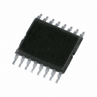
74HC595PW,118 NXP Semiconductors, 74HC595PW,118 Datasheet - Page 20

74HC595PW,118
Manufacturer Part Number
74HC595PW,118
Description
IC SHIFT REGISTER 8BIT 16TSSOP
Manufacturer
NXP Semiconductors
Series
74HCr
Type
Not Requiredr
Datasheet
1.74HC595D118.pdf
(28 pages)
Specifications of 74HC595PW,118
Package / Case
16-TSSOP
Logic Type
Shift Register
Output Type
Standard
Function
Serial to Parallel
Number Of Elements
1
Number Of Bits Per Element
8
Voltage - Supply
2 V ~ 6 V
Operating Temperature
-40°C ~ 125°C
Mounting Type
Surface Mount
Counting Sequence
Serial to Serial/Parallel
Number Of Circuits
1
Logic Family
74HC
Propagation Delay Time
175 ns, 35 ns, 30 ns
Supply Voltage (max)
6 V
Maximum Operating Temperature
+ 125 C
Minimum Operating Temperature
- 40 C
Mounting Style
SMD/SMT
Operating Supply Voltage
2 V to 6 V
Technology
CMOS
Number Of Elements
1
Number Of Bits
8
Logical Function
Shift Register
Operating Supply Voltage (typ)
5V
Package Type
TSSOP
Operating Temp Range
-40C to 125C
Operating Supply Voltage (min)
2V
Operating Supply Voltage (max)
6V
Operating Temperature Classification
Automotive
Mounting
Surface Mount
Pin Count
16
Lead Free Status / RoHS Status
Lead free / RoHS Compliant
Lead Free Status / RoHS Status
Lead free / RoHS Compliant, Lead free / RoHS Compliant
Other names
568-2263-2
74HC595PW-T
935188520118
74HC595PW-T
935188520118
Available stocks
Company
Part Number
Manufacturer
Quantity
Price
Company:
Part Number:
74HC595PW,118
Manufacturer:
NXP Semiconductors
Quantity:
1 250
Philips Semiconductors
2003 Jun 25
handbook, full pagewidth
handbook, full pagewidth
8-bit serial-in, serial or parallel-out shift
register with output latches; 3-state
74HC595: V
74HCT595: V
The shaded areas indicate when the input is permitted to change for predictable output performance.
74HC595: V
74HCT595: V
Fig.10 Waveforms showing the Master Reset (MR) pulse width, the master reset to output (Q7’) propagation
delay and the master reset to shift clock (SH_CP) removal time.
M
M
M
M
= 50%; V
= 50%; V
= 1.3 V; V
= 1.3 V; V
I
I
= GND to V
Fig.9 Waveforms showing the data set-up and hold times for the DS input.
= GND to V
I
I
= GND to 3 V.
= GND to 3 V.
SH_CP input
Q7' output
DS input
CC
CC
SH_CP input
.
.
Q7' output
MR input
V M
V M
t su
V M
t PHL
t h
t W
20
V M
V M
t rem
V M
t su
MLB197
t h
74HC595; 74HCT595
MLB196
Product specification


