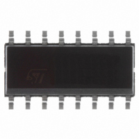
STP08CP05MTR STMicroelectronics, STP08CP05MTR Datasheet

STP08CP05MTR
Specifications of STP08CP05MTR
Available stocks
Related parts for STP08CP05MTR
STP08CP05MTR Summary of contents
Page 1
... Through an external resistor, users can adjust the STP08CP05 output current, controlling in this way the light intensity of LEDs, in addition, user can Table 1. Device summary Order codes STP08CP05B1R STP08CP05MTR STP08CP05TTR STP08CP05XTTR August 2010 DIP-16 TSSOP16 adjust LED’s brightness intensity from 0% to 100% via ...
Page 2
Contents Contents 1 Summary description . . . . . . . . . . . . . . . . . . . . . . . . . . . . . . . . . . . ...
Page 3
STP08CP05 1 Summary description Table 2. Typical current accuracy Output voltage ≥ 1.3 V 1.1 Pin connection and description Figure 1. Connections diagram Note: The exposed pad should be electrically connected to a metal land electrically isolated or connected to ...
Page 4
Block diagram 2 Block diagram Figure 2. Block diagram 4/28 Doc ID 13524 Rev 5 STP08CP05 ...
Page 5
STP08CP05 3 Maximum rating Stressing the device above the rating listed in the “absolute maximum ratings” table may cause permanent damage to the device. these are stress ratings only and operation of the device at these or any other conditions ...
Page 6
Maximum rating 3.3 Recommended operating conditions Table 6. Recommended operating conditions Symbol Parameter V Supply voltage DD V Output voltage O I Output current O I Output current OH I Output current OL V Input voltage IH V Input voltage ...
Page 7
STP08CP05 4 Electrical characteristics °C, unless otherwise specified. DD Table 7. Electrical characteristics Symbol Parameter V Input voltage high level IH V Input voltage low level IL I Output leakage ...
Page 8
Switching characteristics 5 Switching characteristics °C, unless otherwise specified. DD Table 8. Switching characteristics Symbol Parameter Propagation delay time, t CLK-OUTn PLH1 Propagation delay time ...
Page 9
STP08CP05 6 Equivalent circuit and outputs Figure 3. OE terminal Figure 4. LE terminal Figure 5. CLK, SDI terminal Equivalent circuit and outputs Doc ID 13524 Rev 5 9/28 ...
Page 10
Equivalent circuit and outputs Figure 6. SDO terminal 10/28 Doc ID 13524 Rev 5 STP08CP05 ...
Page 11
STP08CP05 7 Truth table and timing diagram 7.1 Truth table Table 9. Truth table Clock Note: OUT0 to OUT7 = ON when OUT0 to OUT7 = OFF when ...
Page 12
Truth table and timing diagram 7.2 Timing diagram Figure 7. Timing diagram 12/28 Doc ID 13524 Rev 5 STP08CP05 ...
Page 13
STP08CP05 Figure 8. Clock, serial-in, serial-out Figure 9. Clock, serial-in, latch, enable, outputs Truth table and timing diagram Doc ID 13524 Rev 5 13/28 ...
Page 14
Truth table and timing diagram Figure 10. Outputs 14/28 Doc ID 13524 Rev 5 STP08CP05 ...
Page 15
STP08CP05 8 Typical characteristics Figure 11. Output current °C, Iset = 3 mA; 5 mA; 10 mA; 20 mA; 50 mA; 80 mA; Max A Table 10. Output current-R Output current (mA) Rext (Ω) Note: Maximum output ...
Page 16
Typical characteristics Figure 12. I SET 910 810 710 610 510 410 310 210 110 Table 11. I SET Vdd (V) I set (mA 16/28 vs drop out voltage (V ) DROP ...
Page 17
STP08CP05 Figure 13. Power dissipation vs temperature package Note: The exposed-pad should be soldered to the PBC to realize the thermal benefits. Figure 14. Current precision between outputs vs output current 5.5 4.5 3.5 2.5 1.5 0 ...
Page 18
Test circuit 9 Test circuit Figure 15. DC characteristics Figure 16. AC characteristics 18/28 Doc ID 13524 Rev 5 STP08CP05 ...
Page 19
STP08CP05 Figure 17. Typical application schematic Doc ID 13524 Rev 5 Test circuit 19/28 ...
Page 20
Package mechanical data 10 Package mechanical data In order to meet environmental requirements, ST offers these devices in different grades of ® ECOPACK packages, depending on their level of environmental compliance. ECOPACK specifications, grade definitions and product status are available ...
Page 21
STP08CP05 Figure 18. DIP-16 mechanical data DIM. MIN. a1 0. Plastic DIP-16 (0.25) MECHANICAL DATA mm. TYP MAX. 1.65 0.5 0.25 20 8.5 2.54 17.78 7.1 5.1 3.3 ...
Page 22
Package mechanical data Figure 19. TSSOP16 mechanical data DIM. MIN 0.05 A2 0.8 b 0.19 c 0.09 D 4.9 E 6 0˚ PIN 1 IDENTIFICATION 1 22/28 TSSOP16 ...
Page 23
STP08CP05 Figure 20. TSSOP16 exposed pad mechanical data DIM. MIN 0.8 b 0.19 c 0.09 D 4.9 D1 2.7 E 6 0° L 0.45 TSSOP16 EXPOSED PAD MECHANICAL DATA mm. TYP ...
Page 24
Package mechanical data Figure 21. TSSOP16 tape and reel Tape & Reel TSSOP16 MECHANICAL DATA DIM. MIN 12 6.7 Bo 5.3 Ko 1.6 Po 3.9 P 7.9 24/28 mm. TYP MAX. MIN. ...
Page 25
STP08CP05 Figure 22. SO-16 mechanical data DIM. MIN 0 0. 9 3.8 G 4 SO-16 MECHANICAL DATA mm. TYP MAX. MIN. 1.75 ...
Page 26
Package mechanical data Figure 23. SO-16 tape and reel DIM. MIN 12 6.45 Bo 10.3 Ko 2.1 Po 3.9 P 7.9 26/28 Tape & Reel SO-16 MECHANICAL DATA mm. TYP MAX. 330 ...
Page 27
STP08CP05 11 Revision history Table 12. Document revision history Date 23-May-2007 28-Jun-2007 12-Mar-2008 07-Aug-2008 27-Aug-2010 Revision 1 First release 2 Updated Table 7 on page 7 Updated Table 8 on page 8 3 Figure 12 on page 16 4 Updated ...
Page 28
... Information in this document is provided solely in connection with ST products. STMicroelectronics NV and its subsidiaries (“ST”) reserve the right to make changes, corrections, modifications or improvements, to this document, and the products and services described herein at any time, without notice. All ST products are sold pursuant to ST’s terms and conditions of sale. ...


