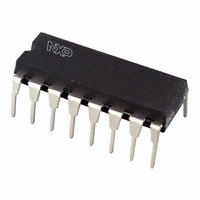
N74F259N,602 NXP Semiconductors, N74F259N,602 Datasheet - Page 2

N74F259N,602
Manufacturer Part Number
N74F259N,602
Description
IC LATCH ADDRESSABLE 31MA 16DIP
Manufacturer
NXP Semiconductors
Series
74Fr
Datasheet
1.N74F259D602.pdf
(12 pages)
Specifications of N74F259N,602
Logic Type
D-Type, Addressable
Circuit
1:8
Output Type
Standard
Voltage - Supply
4.5 V ~ 5.5 V
Independent Circuits
1
Delay Time - Propagation
5ns
Current - Output High, Low
1mA, 20mA
Operating Temperature
0°C ~ 70°C
Mounting Type
Through Hole
Package / Case
16-DIP (0.300", 7.62mm)
Lead Free Status / RoHS Status
Lead free / RoHS Compliant
Other names
568-1724-5
933731290602
N74F259N
933731290602
N74F259N
Philips Semiconductors
FEATURES
DESCRIPTION
The 74F259 addressable latch has four distinct modes of operation
which are selectable by controlling the Master Reset (MR) and
Enable (E) inputs (see Function Table). In the addressable latch
mode, data at the Data inputs is written into the addressed latches.
The addressed latches will follow the Data input with all
unaddressed latches remaining in their previous states. In the store
mode, all latches remain in their previous states and are unaffected
by the Data or Address inputs. To eliminate the possibility of entering
erroneous data in the latches, the enable should be held High
(inactive) while the address lines are changing. In the 1-of-8
decoding or demultiplexing mode (MR=E=Low), addressed outputs
will follow the level of the Data input, with all other outputs Low. In
the Master Reset mode, all outputs are Low and unaffected by the
Address and Data inputs.
INPUT AND OUTPUT LOADING AND FAN-OUT TABLE
NOTE:
One (1.0) FAST unit load is defined as: 20 A in the High state and 0.6mA in the Low state.
1989 Apr 11
Combines demultiplexer and 8-bit latch
Serial-to-parallel capability
Output from each storage bit available
Random (addressable) data entry
Easily expandable
Common reset input
Useful as 1-of-8 active-High decoder
Latch
A0, A1, A2
Q0 – Q7
PINS
MR
D
E
Data input
Address inputs
Enable input (active Low)
Master Reset inputs (active Low)
Data outputs
DESCRIPTION
2
PIN CONFIGURATION
ORDERING INFORMATION
16-pin plastic DIP
16-pin plastic SO
DESCRIPTION
TYPE
74F259
PROPAGATION
TYPICAL
GND
DELAY
Q0
Q1
Q2
Q3
A0
A1
A2
7.5ns
COMMERCIAL RANGE
T
1
2
3
4
5
6
7
8
amb
V
HIGH/LOW
ORDER CODE
74F (U.L.)
CC
1.0/1.0
1.0/1.0
1.0/1.0
1.0/1.0
N74F259N
N74F259D
= 0 C to +70 C
50/33
= 5V 10%,
SF00823
16
15
14
13
12
11
10
9
CURRENT (TOTAL)
TYPICAL SUPPLY
V
MR
E
D
Q7
Q6
Q5
Q4
CC
Product specification
LOAD VALUE
1.0mA/20mA
20 A/0.6mA
20 A/0.6mA
20 A/0.6mA
20 A/0.6mA
31mA
853–0362 06316
HIGH/LOW
PKG DWG #
74F259
SOT109-1
SOT38-4


