74HCT563N,652 NXP Semiconductors, 74HCT563N,652 Datasheet - Page 2
74HCT563N,652
Manufacturer Part Number
74HCT563N,652
Description
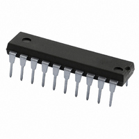
IC OCT D TRANSP LATCH INV 20DIP
Manufacturer
NXP Semiconductors
Series
74HCTr
Datasheet
1.74HCT563DB118.pdf
(7 pages)
Specifications of 74HCT563N,652
Logic Type
D-Type Transparent Latch
Package / Case
20-DIP (0.300", 7.62mm)
Circuit
8:8
Output Type
Tri-State
Voltage - Supply
4.5 V ~ 5.5 V
Independent Circuits
1
Delay Time - Propagation
18ns
Operating Temperature
-40°C ~ 125°C
Mounting Type
Through Hole
Number Of Circuits
8
Logic Family
HCT
Polarity
Inverting
High Level Output Current
- 6 mA
Low Level Output Current
6 mA
Propagation Delay Time
16 ns
Supply Voltage (max)
5.5 V
Supply Voltage (min)
4.5 V
Maximum Operating Temperature
+ 125 C
Minimum Operating Temperature
- 40 C
Mounting Style
Through Hole
Current - Output High, Low
-
Lead Free Status / RoHS Status
Lead free / RoHS Compliant
Current - Output High, Low
-
Lead Free Status / Rohs Status
Lead free / RoHS Compliant
Other names
74HCT563N
74HCT563N
933670920652
74HCT563N
933670920652


Philips Semiconductors
FEATURES
GENERAL DESCRIPTION
The 74HC/HCT563 are high-speed
Si-gate CMOS devices and are pin
compatible with low power Schottky
QUICK REFERENCE DATA
GND = 0 V; T
Notes
1. C
2. For HC the condition is V
ORDERING INFORMATION
See
December 1990
SYMBOL
t
C
C
PHL/
3-state inverting outputs for bus
oriented applications
Inputs and outputs on opposite
sides of package allowing easy
interface with microprocessor
Common 3-state output enable
input
Output capability: bus driver
I
Octal D-type transparent latch; 3-state;
inverting
I
PD
CC
f
f
C
V
for HCT the condition is V
i
o
“74HC/HCT/HCU/HCMOS Logic Package Information”
CC
PD
= input frequency in MHz
L
t
category: MSI
= output frequency in MHz
(C
PLH
= output load capacitance in pF
P
= supply voltage in V
is used to determine the dynamic power dissipation (P
L
D
= C
V
amb
CC
PD
PARAMETER
propagation delay D
input capacitance
power dissipation capacitance per latch
2
= 25 C; t
V
f
o
CC
) = sum of outputs
2
f
r
i
= t
I
I
f
= GND to V
= GND to V
= 6 ns
(C
n
L
, LE to Q
V
CC
TTL (LSTTL). They are specified in
compliance with JEDEC standard no.
7A.
The 74HC/HCT563 are octal D-type
transparent latches featuring
separate D-type inputs for each latch
and inverting 3-state outputs for bus
oriented applications.
A latch enable (LE) input and an
output enable (OE) input are common
to all latches.
The “563” is functionally identical to
the “573”, but has inverted outputs.
The “563” consists of eight D-type
transparent latches with 3-state
inverting outputs. The LE and OE are
2
CC
CC
n
f
o
1.5 V
) where:
CONDITIONS
C
notes 1 and 2
2
.
L
= 15 pF; V
D
in W):
CC
= 5 V
common to all latches.
When LE is HIGH, data at the D
inputs enter the latches. In this
condition the latches are transparent,
i.e. a latch output will change state
each time its corresponding D-input
changes.
When LE is LOW the latches store the
information that was present at the
D-inputs a set-up time preceding the
HIGH-to-LOW transition of LE.
When OE is LOW, the contents of the
8 latches are available at the outputs.
When OE is HIGH, the outputs go to
the high impedance OFF-state.
Operation of the OE input does not
affect the state of the latches.
HC
14
3.5
19
TYPICAL
74HC/HCT563
Product specification
HCT
16
3.5
19
UNIT
ns
pF
pF
n
Related parts for 74HCT563N,652
Image
Part Number
Description
Manufacturer
Datasheet
Request
R

Part Number:
Description:
Octal D-type Transparent Latch; 3-state; Inverting
Manufacturer:
NXP Semiconductors
Datasheet:

Part Number:
Description:
IC BUFF/DVR TRI-ST DUAL 20DIP
Manufacturer:
Fairchild Semiconductor
Datasheet:

Part Number:
Description:
IC BUS TRANSCVR 3-ST 8BIT 20DIP
Manufacturer:
ON Semiconductor
Datasheet:

Part Number:
Description:
IC TRANSCEIVER 3-ST 8BIT 20SOIC
Manufacturer:
Fairchild Semiconductor
Datasheet:

Part Number:
Description:
IC BUFFER NONINV QUAD 3ST 14SOIC
Manufacturer:
ON Semiconductor
Datasheet:
Part Number:
Description:
IC BUFFER NONINV QUAD 3ST 14SOIC
Manufacturer:
ON Semiconductor
Datasheet:

Part Number:
Description:
IC BUS TRANSCVR 3-ST 8BIT 20SOIC
Manufacturer:
ON Semiconductor
Datasheet:

Part Number:
Description:
IC BUFF/DVR TRI-ST 8BIT 20SOIC
Manufacturer:
ON Semiconductor
Datasheet:

Part Number:
Description:
IC FLIP FLOP OCT D 3ST 20TSSOP
Manufacturer:
Fairchild Semiconductor
Datasheet:

Part Number:
Description:
IC FLIP FLOP OCTAL D 20-DIP
Manufacturer:
STMicroelectronics
Datasheet:

Part Number:
Description:
IC FLIP FLOP DUAL D-TYPE 14-SOIC
Manufacturer:
Fairchild Semiconductor
Datasheet:
Part Number:
Description:
IC FLIP FLOP OCTAL D 20-SOIC
Manufacturer:
Fairchild Semiconductor
Datasheet:

Part Number:
Description:
IC FLIP FLOP OCT D 3ST 20-SOIC
Manufacturer:
ON Semiconductor
Datasheet:

Part Number:
Description:
IC INVERT HEX SCHM TRIG 14-SOIC
Manufacturer:
ON Semiconductor
Datasheet:

Part Number:
Description:
IC INVERTER HEX LSTTL IN 14TSSOP
Manufacturer:
ON Semiconductor
Datasheet: