74ABT373ADB,118 NXP Semiconductors, 74ABT373ADB,118 Datasheet - Page 5
74ABT373ADB,118
Manufacturer Part Number
74ABT373ADB,118
Description
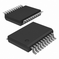
IC OCTAL TRANSP LATCH 3ST 20SSOP
Manufacturer
NXP Semiconductors
Series
74ABTr
Datasheet
1.74ABT373AD118.pdf
(11 pages)
Specifications of 74ABT373ADB,118
Logic Type
D-Type Transparent Latch
Circuit
8:8
Output Type
Tri-State
Voltage - Supply
4.5 V ~ 5.5 V
Independent Circuits
1
Delay Time - Propagation
3.6ns
Current - Output High, Low
32mA, 64mA
Operating Temperature
-40°C ~ 85°C
Mounting Type
Surface Mount
Package / Case
20-SSOP
Lead Free Status / RoHS Status
Lead free / RoHS Compliant
Other names
74ABT373ADB-T
74ABT373ADB-T
935191310118
74ABT373ADB-T
935191310118


1. Not more than one output should be tested at a time, and the duration of the test should not exceed one second.
2. This is the increase in supply current for each input at 3.4V.
3. For valid test results, data must not be loaded into the flip-flops (or latches) after applying the power.
Philips Semiconductors
DC ELECTRICAL CHARACTERISTICS
NOTES:
AC CHARACTERISTICS
GND = 0V, t
1995 Feb 17
SYMBOL
SYMBOL
t
t
t
t
t
t
t
t
PLH
PHL
PLH
PHL
PZH
PZL
PHZ
PLZ
Octal transparent latch (3-State)
I
PU
V
I
I
V
I
I
I
I
I
V
V
OFF
OZH
CEX
CCH
CCL
CCZ
OZL
RST
I
I
OH
OL
I
/I
O
CC
IK
I
PD
R
Input clamp voltage
High-level output voltage
Low-level output voltage
Power-up output low
voltage
Input leakage current
Power-off leakage current
Power-up/down 3-State
output current
3-State output High current
3-State output Low current
Output High leakage current
Output current
Quiescent supply current
Quiescent su
Additional supply current per
input pin
= t
Propagation delay
Dn to Qn
Propagation delay
E to Qn
Output enable time
to High and Low level
Output disable time
from High and Low level
F
= 2.5ns, C
3
PARAMETER
PARAMETER
2
1
L
ly current
= 50pF, R
L
= 500
V
V
V
V
V
V
V
V
V
= GND or V
V
V
V
V
V
V
V
V
V
other inputs at V
CC
CC
CC
CC
CC
CC
CC
CC
CC
CC
CC
CC
CC
CC
CC
CC
I
CC
= GND or V
= 4.5V; I
= 4.5V; I
= 5.0V; I
= 4.5V; I
= 4.5V; I
= 5.5V; I
= 5.5V; V
= 0.0V; V
= 2.0V; V
= 5.5V; V
= 5.5V; V
= 5.5V; V
= 5.5V; V
= 5.5V; Outputs High, V
= 5.5V; Outputs Low, V
= 5.5V; Outputs 3-State;
= 5.5V; one input at 3.4V,
WAVEFORM
CC
2
1
4
5
4
5
TEST CONDITIONS
IK
OH
OH
OH
OL
O
I
O
O
O
O
O
O
CC
= 1mA; V
= GND or 5.5V
= –18mA
or V
= 0.5V; V
= 2.7V; V
= 0.5V; V
= 5.5V; V
= 2.5V
= 64mA; V
= –32mA; V
CC
= –3mA; V
= –3mA; V
or GND
I
4.5V
I
OE
I
I
I
= GND or V
5
= V
= V
= GND or V
I
I
I
= V
I
= V
= V
I
I
= Don’t Care V
= GND or V
= V
= GND or V
IL
IL
Min
1.4
1.4
1.4
1.9
1.2
2.1
1.3
1.2
IL
IL
IL
or V
or V
IL
or V
or V
or V
or V
IH
IH
T
CC
IH
V
IH
IH
CC
amb
IH
CC
CC
CC
Typ
3.2
3.6
3.2
3.7
3.1
4.2
3.4
3.0
= +5.0V
= +25
1
o
Min
–50
2.5
3.0
2.0
C
LIMITS
T
Max
amb
4.2
4.7
4.2
4.8
4.2
5.2
4.6
4.1
–100
–0.9
0.13
–0.1
Typ
100
100
2.9
3.4
2.4
0.3
0.01
0.1
5.0
0.5
= +25 C
24
5.0
5.0
V
LIMITS
CC
Min
1.4
1.4
1.4
1.9
1.2
2.1
1.3
1.2
–180
Max
–1.2
0.55
0.55
–50
250
250
T
1.5
100
50
50
30
1.0
50
amb
= +5.0V 0.5V
+85
= -40 to
o
T
74ABT373A
C
Min
–50
amb
2.5
3.0
2.0
to +85 C
Max
4.7
5.1
4.8
5.1
5.1
5.7
5.1
4.3
Product specification
= –40 C
–180
Max
–1.2
0.55
0.55
–50
250
250
1.5
100
50
50
30
1.0
50
UNIT
ns
ns
ns
ns
UNIT
mA
mA
mA
V
V
V
V
V
V
A
A
A
A
A
A
A
A
Related parts for 74ABT373ADB,118
Image
Part Number
Description
Manufacturer
Datasheet
Request
R

Part Number:
Description:
NXP Semiconductors designed the LPC2420/2460 microcontroller around a 16-bit/32-bitARM7TDMI-S CPU core with real-time debug interfaces that include both JTAG andembedded trace
Manufacturer:
NXP Semiconductors
Datasheet:

Part Number:
Description:
NXP Semiconductors designed the LPC2458 microcontroller around a 16-bit/32-bitARM7TDMI-S CPU core with real-time debug interfaces that include both JTAG andembedded trace
Manufacturer:
NXP Semiconductors
Datasheet:
Part Number:
Description:
NXP Semiconductors designed the LPC2468 microcontroller around a 16-bit/32-bitARM7TDMI-S CPU core with real-time debug interfaces that include both JTAG andembedded trace
Manufacturer:
NXP Semiconductors
Datasheet:
Part Number:
Description:
NXP Semiconductors designed the LPC2470 microcontroller, powered by theARM7TDMI-S core, to be a highly integrated microcontroller for a wide range ofapplications that require advanced communications and high quality graphic displays
Manufacturer:
NXP Semiconductors
Datasheet:
Part Number:
Description:
NXP Semiconductors designed the LPC2478 microcontroller, powered by theARM7TDMI-S core, to be a highly integrated microcontroller for a wide range ofapplications that require advanced communications and high quality graphic displays
Manufacturer:
NXP Semiconductors
Datasheet:
Part Number:
Description:
The Philips Semiconductors XA (eXtended Architecture) family of 16-bit single-chip microcontrollers is powerful enough to easily handle the requirements of high performance embedded applications, yet inexpensive enough to compete in the market for hi
Manufacturer:
NXP Semiconductors
Datasheet:
Part Number:
Description:
The XA-S3 device is a member of Philips Semiconductors? XA(eXtended Architecture) family of high performance 16-bitsingle-chip microcontrollers
Manufacturer:
NXP Semiconductors
Datasheet:

Part Number:
Description:
The NXP BlueStreak LH75401/LH75411 family consists of two low-cost 16/32-bit System-on-Chip (SoC) devices
Manufacturer:
NXP Semiconductors
Datasheet:
Part Number:
Description:
The NXP LPC3130/3131 combine an 180 MHz ARM926EJ-S CPU core, high-speed USB2
Manufacturer:
NXP Semiconductors
Datasheet:
Part Number:
Description:
The NXP LPC3141 combine a 270 MHz ARM926EJ-S CPU core, High-speed USB 2
Manufacturer:
NXP Semiconductors
Part Number:
Description:
The NXP LPC3143 combine a 270 MHz ARM926EJ-S CPU core, High-speed USB 2
Manufacturer:
NXP Semiconductors

Part Number:
Description:
The NXP LPC3152 combines an 180 MHz ARM926EJ-S CPU core, High-speed USB 2
Manufacturer:
NXP Semiconductors
Part Number:
Description:
The NXP LPC3154 combines an 180 MHz ARM926EJ-S CPU core, High-speed USB 2
Manufacturer:
NXP Semiconductors

Part Number:
Description:
Standard level N-channel enhancement mode Field-Effect Transistor (FET) in a plastic package using NXP High-Performance Automotive (HPA) TrenchMOS technology
Manufacturer:
NXP Semiconductors
Datasheet: