74LVT573PW,112 NXP Semiconductors, 74LVT573PW,112 Datasheet - Page 5
74LVT573PW,112
Manufacturer Part Number
74LVT573PW,112
Description
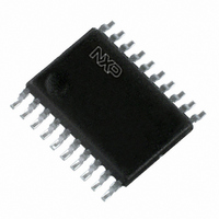
IC OCTAL D TRANSP LATCH 20TSSOP
Manufacturer
NXP Semiconductors
Series
74LVTr
Datasheet
1.74LVT573DB112.pdf
(16 pages)
Specifications of 74LVT573PW,112
Logic Type
D-Type Transparent Latch
Circuit
8:8
Output Type
Tri-State
Voltage - Supply
2.7 V ~ 3.6 V
Independent Circuits
1
Delay Time - Propagation
6.3ns
Current - Output High, Low
32mA, 64mA
Operating Temperature
-40°C ~ 85°C
Mounting Type
Surface Mount
Package / Case
20-TSSOP
Lead Free Status / RoHS Status
Lead free / RoHS Compliant
Other names
74LVT573PW
74LVT573PW
935176360112
74LVT573PW
935176360112


NXP Semiconductors
Table 4.
In accordance with the Absolute Maximum Rating System (IEC 60134). Voltages are referenced to GND (ground = 0 V).
[1]
[2]
[3]
8. Recommended operating conditions
Table 5.
9. Static characteristics
Table 6.
At recommended operating conditions; voltages are referenced to GND (ground = 0 V).
74LVT573_4
Product data sheet
Symbol
T
T
P
Symbol
V
V
V
V
I
I
T
Symbol Parameter
V
V
V
V
OH
OL
stg
j
amb
t/ V
tot
CC
I
IH
IL
IK
OH
OL
OL(pu)
The input and output negative voltage ratings may be exceeded if the input and output clamp current ratings are observed.
The performance capability of a high-performance integrated circuit in conjunction with its thermal environment can create junction
temperatures which are detrimental to reliability.
For SO20 packages: above 70 C derate linearly with 8 mW/K.
For SSOP20 and TSSOP20 packages: above 60 C derate linearly with 5.5 mW/K.
For DHVQFN20 packages: above 60 C derate linearly with 4.5 mW/K.
input clamping voltage
HIGH-level output voltage
LOW-level output voltage
power-up LOW-level
output voltage
Parameter
supply voltage
input voltage
HIGH-level input voltage
LOW-level input voltage
HIGH-level output current
LOW-level output current
ambient temperature
input transition rise and fall rate
Limiting values
Recommended operating conditions
Static characteristics
Parameter
storage temperature
junction temperature
total power dissipation
…continued
Conditions
V
V
I
V
V
V
V
V
V
V
V
V
Conditions
T
OH
Conditions
current duty cycle
in free air
outputs enabled
CC
CC
CC
CC
CC
CC
CC
CC
CC
CC
I
amb
Rev. 04 — 15 September 2008
= GND or V
= 100 A
= 2.7 V; I
= 2.7 V to 3.6 V;
= 2.7 V; I
= 3.0 V; I
= 2.7 V; I
= 2.7 V; I
= 3.0 V I
= 3.0 V I
= 3.0 V I
= 3.6 V; I
= 40 C to +85 C
OL
OL
OL
IK
OH
OH
OL
OL
O
CC
= 1 mA;
= 18 mA
= 16 mA
= 32 mA
= 64 mA
= 100 A
= 24 mA
= 8 mA
= 32 mA
50 %; f
3.3 V octal D-type transparent latch; (3-state)
i
1 kHz
[2]
V
[2]
[3]
CC
T
Min
2.7
0
2.0
-
-
-
-
-
Min
2.4
2.0
amb
1.2
40
-
-
-
-
-
-
Min
-
-
65
0.2 V
= 40 C to +85 C
Typ
-
-
-
-
-
-
-
-
-
CC
Typ
0.25
0.13
74LVT573
2.5
2.2
0.1
0.3
0.3
0.4
0.9
Max
+150
150
500
© NXP B.V. 2008. All rights reserved.
[1]
0.1
Max
3.6
5.5
-
0.8
32
64
+85
10
32
Max
0.55
0.55
0.2
0.5
0.4
0.5
-
-
-
-
Unit
mW
C
C
Unit
mA
mA
V
V
V
V
mA
ns/V
5 of 16
Unit
V
V
V
V
V
V
V
V
V
V
C
Related parts for 74LVT573PW,112
Image
Part Number
Description
Manufacturer
Datasheet
Request
R

Part Number:
Description:
3.3V Octal D-type transparent latch 3-State
Manufacturer:
PHILIPS [NXP Semiconductors]
Datasheet:

Part Number:
Description:
NXP Semiconductors designed the LPC2420/2460 microcontroller around a 16-bit/32-bitARM7TDMI-S CPU core with real-time debug interfaces that include both JTAG andembedded trace
Manufacturer:
NXP Semiconductors
Datasheet:

Part Number:
Description:
NXP Semiconductors designed the LPC2458 microcontroller around a 16-bit/32-bitARM7TDMI-S CPU core with real-time debug interfaces that include both JTAG andembedded trace
Manufacturer:
NXP Semiconductors
Datasheet:
Part Number:
Description:
NXP Semiconductors designed the LPC2468 microcontroller around a 16-bit/32-bitARM7TDMI-S CPU core with real-time debug interfaces that include both JTAG andembedded trace
Manufacturer:
NXP Semiconductors
Datasheet:
Part Number:
Description:
NXP Semiconductors designed the LPC2470 microcontroller, powered by theARM7TDMI-S core, to be a highly integrated microcontroller for a wide range ofapplications that require advanced communications and high quality graphic displays
Manufacturer:
NXP Semiconductors
Datasheet:
Part Number:
Description:
NXP Semiconductors designed the LPC2478 microcontroller, powered by theARM7TDMI-S core, to be a highly integrated microcontroller for a wide range ofapplications that require advanced communications and high quality graphic displays
Manufacturer:
NXP Semiconductors
Datasheet:
Part Number:
Description:
The Philips Semiconductors XA (eXtended Architecture) family of 16-bit single-chip microcontrollers is powerful enough to easily handle the requirements of high performance embedded applications, yet inexpensive enough to compete in the market for hi
Manufacturer:
NXP Semiconductors
Datasheet:
Part Number:
Description:
The XA-S3 device is a member of Philips Semiconductors? XA(eXtended Architecture) family of high performance 16-bitsingle-chip microcontrollers
Manufacturer:
NXP Semiconductors
Datasheet:

Part Number:
Description:
The NXP BlueStreak LH75401/LH75411 family consists of two low-cost 16/32-bit System-on-Chip (SoC) devices
Manufacturer:
NXP Semiconductors
Datasheet:
Part Number:
Description:
The NXP LPC3130/3131 combine an 180 MHz ARM926EJ-S CPU core, high-speed USB2
Manufacturer:
NXP Semiconductors
Datasheet:
Part Number:
Description:
The NXP LPC3141 combine a 270 MHz ARM926EJ-S CPU core, High-speed USB 2
Manufacturer:
NXP Semiconductors
Part Number:
Description:
The NXP LPC3143 combine a 270 MHz ARM926EJ-S CPU core, High-speed USB 2
Manufacturer:
NXP Semiconductors

Part Number:
Description:
The NXP LPC3152 combines an 180 MHz ARM926EJ-S CPU core, High-speed USB 2
Manufacturer:
NXP Semiconductors
Part Number:
Description:
The NXP LPC3154 combines an 180 MHz ARM926EJ-S CPU core, High-speed USB 2
Manufacturer:
NXP Semiconductors