74HCT373N,652 NXP Semiconductors, 74HCT373N,652 Datasheet - Page 15
74HCT373N,652
Manufacturer Part Number
74HCT373N,652
Description
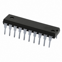
IC LATCH TRANSP OCT D 3ST 20DIP
Manufacturer
NXP Semiconductors
Series
74HCTr
Type
D-Typer
Datasheet
1.74HC373PW118.pdf
(26 pages)
Specifications of 74HCT373N,652
Logic Type
D-Type Transparent Latch
Package / Case
20-DIP (0.300", 7.62mm)
Circuit
8:8
Output Type
Tri-State
Voltage - Supply
4.5 V ~ 5.5 V
Independent Circuits
1
Delay Time - Propagation
33ns
Current - Output High, Low
6mA, 6mA
Operating Temperature
-40°C ~ 125°C
Mounting Type
Through Hole
Number Of Circuits
8
Logic Family
74HCT
Polarity
Non-Inverting
High Level Output Current
- 6 mA
Low Level Output Current
6 mA
Propagation Delay Time
14 ns
Supply Voltage (max)
5.5 V
Supply Voltage (min)
4.5 V
Maximum Operating Temperature
+ 125 C
Minimum Operating Temperature
- 40 C
Mounting Style
Through Hole
Number Of Bits
8
Number Of Elements
1
Latch Mode
Transparent
Technology
CMOS
Package Type
PDIP
Operating Supply Voltage (typ)
5V
Operating Supply Voltage (min)
4.5V
Operating Supply Voltage (max)
5.5V
Operating Temp Range
-40C to 125C
Operating Temperature Classification
Automotive
Mounting
Through Hole
Pin Count
20
Lead Free Status / RoHS Status
Lead free / RoHS Compliant
Lead Free Status / RoHS Status
Lead free / RoHS Compliant, Lead free / RoHS Compliant
Other names
568-1541-5
74HCT373N
933670850652
74HCT373N
933670850652


NXP Semiconductors
Table 9.
Voltages are referenced to GND (ground = 0 V); C
[1]
[2]
[3]
[4]
[5]
11. Waveforms
74HC_HCT373
Product data sheet
Symbol Parameter
t
h
Fig 8.
Fig 9.
t
t
t
t
C
P
f
f
C
V
N = number of inputs switching;
∑(C
pd
en
dis
t
i
o
D
CC
PD
= input frequency in MHz;
L
is the same as t
= output frequency in MHz;
is the same as t
is the same as t
= output load capacitance in pF;
= C
is the same as t
L
is used to determine the dynamic power dissipation (P
= supply voltage in V;
× V
hold time Dn to LE
Measurement points are given in
Propagation delay input (Dn) to output (Qn) and transition time output (Qn)
Measurement points are given in
Pulse width latch enable input (LE), propagation delay (LE) to output (Qn) and transition time output (Qn)
PD
Dynamic characteristics 74HCT373
CC
× V
2
× f
CC
o
2
) = sum of outputs.
× f
THL
PLH
PZH
PLZ
i
× N + ∑(C
and t
and t
and t
and t
TLH
PHL
PZL
PHZ
.
L
.
.
.
× V
Qn output
Qn output
LE input
Dn input
CC
2
× f
Table
Table
o
All information provided in this document is subject to legal disclaimers.
) where:
10.
10.
Conditions
Dn to LE; see
Rev. 4 — 3 September 2010
t
…continued
L
THL
V
V
90 %
= 50 pF unless otherwise specified; for test circuit see
M
t
CC
PHL
V
t
t
W
= 4.5 V
M
TLH
t
10 %
D
PLH
in μW).
V
V
M
M
10 %
Figure 11
90 %
t
TLH
t
THL
t
t
PHL
PLH
74HC373; 74HCT373
Octal D-type transparent latch; 3-state
001aae082
001aae083
Min
4
Typ
-
© NXP B.V. 2010. All rights reserved.
Figure
Max
-
12.
Unit
ns
15 of 26
Related parts for 74HCT373N,652
Image
Part Number
Description
Manufacturer
Datasheet
Request
R

Part Number:
Description:
Manufacturer:
NXP Semiconductors
Datasheet:

Part Number:
Description:
IC BUFF/DVR TRI-ST DUAL 20DIP
Manufacturer:
Fairchild Semiconductor
Datasheet:

Part Number:
Description:
IC BUS TRANSCVR 3-ST 8BIT 20DIP
Manufacturer:
ON Semiconductor
Datasheet:

Part Number:
Description:
IC TRANSCEIVER 3-ST 8BIT 20SOIC
Manufacturer:
Fairchild Semiconductor
Datasheet:

Part Number:
Description:
IC BUFFER NONINV QUAD 3ST 14SOIC
Manufacturer:
ON Semiconductor
Datasheet:
Part Number:
Description:
IC BUFFER NONINV QUAD 3ST 14SOIC
Manufacturer:
ON Semiconductor
Datasheet:

Part Number:
Description:
IC BUS TRANSCVR 3-ST 8BIT 20SOIC
Manufacturer:
ON Semiconductor
Datasheet:

Part Number:
Description:
IC BUFF/DVR TRI-ST 8BIT 20SOIC
Manufacturer:
ON Semiconductor
Datasheet:

Part Number:
Description:
IC FLIP FLOP OCT D 3ST 20TSSOP
Manufacturer:
Fairchild Semiconductor
Datasheet:

Part Number:
Description:
IC FLIP FLOP OCTAL D 20-DIP
Manufacturer:
STMicroelectronics
Datasheet:

Part Number:
Description:
IC FLIP FLOP DUAL D-TYPE 14-SOIC
Manufacturer:
Fairchild Semiconductor
Datasheet:
Part Number:
Description:
IC FLIP FLOP OCTAL D 20-SOIC
Manufacturer:
Fairchild Semiconductor
Datasheet:

Part Number:
Description:
IC FLIP FLOP OCT D 3ST 20-SOIC
Manufacturer:
ON Semiconductor
Datasheet:

Part Number:
Description:
IC INVERT HEX SCHM TRIG 14-SOIC
Manufacturer:
ON Semiconductor
Datasheet:

Part Number:
Description:
IC INVERTER HEX LSTTL IN 14TSSOP
Manufacturer:
ON Semiconductor
Datasheet: