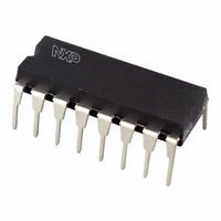
74HC259N,652 NXP Semiconductors, 74HC259N,652 Datasheet - Page 11

74HC259N,652
Manufacturer Part Number
74HC259N,652
Description
IC ADDRESSABLE LATCH 8BIT 16DIP
Manufacturer
NXP Semiconductors
Series
74HCr
Type
D-Typer
Specifications of 74HC259N,652
Logic Type
D-Type, Addressable
Package / Case
16-DIP (0.300", 7.62mm)
Circuit
1:8
Output Type
Standard
Voltage - Supply
2 V ~ 6 V
Independent Circuits
1
Delay Time - Propagation
17ns
Current - Output High, Low
5.2mA, 5.2mA
Operating Temperature
-40°C ~ 125°C
Mounting Type
Through Hole
Number Of Circuits
1
Logic Family
74HC
Polarity
Non-Inverting
High Level Output Current
- 5.2 mA
Low Level Output Current
5.2 mA
Propagation Delay Time
185 ns at 2 V, 37 ns at 4.5 V, 31 ns at 6 V
Supply Voltage (max)
6 V
Supply Voltage (min)
2 V
Maximum Operating Temperature
+ 125 C
Minimum Operating Temperature
- 40 C
Mounting Style
Through Hole
Number Of Bits
8
Number Of Elements
1
Latch Mode
Addressable
Technology
CMOS
Package Type
PDIP
Operating Supply Voltage (typ)
5V
Operating Supply Voltage (min)
2V
Operating Supply Voltage (max)
6V
Operating Temp Range
-40C to 125C
Operating Temperature Classification
Automotive
Mounting
Through Hole
Pin Count
16
Lead Free Status / RoHS Status
Lead free / RoHS Compliant
Lead Free Status / RoHS Status
Lead free / RoHS Compliant, Lead free / RoHS Compliant
Other names
568-1427-5
74HC259N
933669560652
74HC259N
933669560652
Philips Semiconductors
PACKAGE OUTLINES
See
December 1990
8-bit addressable latch
(1) HC : V
The shaded areas indicate when the input is
permitted to change for predictable output
performance.
(1) HC : V
The shaded areas indicate when the input is
permitted to change for predictable output
performance.
(1) HC : V
“74HC/HCT/HCU/HCMOS Logic Package Outlines”
HCT: V
HCT: V
HCT: V
M
M
M
M
M
M
Fig.9 Waveforms showing the conditional reset input (MR) to output (Q
= 50%; V
= 50%; V
= 50%; V
= 1.3 V; V
= 1.3 V; V
= 1.3 V; V
Fig.11 Waveforms showing the address set-up and hold times for A
Fig.10 Waveforms showing the data set-up and hold times for the D input to LE input.
I
I
I
I
I
I
= GND to V
= GND to V
= GND to V
= GND to 3 V.
= GND to 3 V.
= GND to 3 V.
CC
CC
CC
.
.
.
.
11
n
n
) propagation delays.
inputs to LE input.
74HC/HCT259
Product specification


