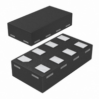
74LVC1G99GT,115 NXP Semiconductors, 74LVC1G99GT,115 Datasheet - Page 14

74LVC1G99GT,115
Manufacturer Part Number
74LVC1G99GT,115
Description
IC CONFIG MULTI-FUNC GATE 8-XSON
Manufacturer
NXP Semiconductors
Series
74LVCr
Datasheet
1.74LVC1G99GT115.pdf
(32 pages)
Specifications of 74LVC1G99GT,115
Number Of Circuits
1
Package / Case
8-XSON
Logic Type
Configurable Multiple Function
Number Of Inputs
4
Schmitt Trigger Input
Yes
Output Type
Single-Ended
Current - Output High, Low
32mA, 32mA
Voltage - Supply
1.65 V ~ 5.5 V
Operating Temperature
-40°C ~ 125°C
Mounting Type
Surface Mount
Product
MUX Gates
Logic Family
74LVC
High Level Output Current
- 32 mA
Low Level Output Current
32 mA
Propagation Delay Time
5.4 ns
Supply Voltage (max)
5.5 V
Supply Voltage (min)
1.65 V
Maximum Operating Temperature
+ 125 C
Mounting Style
SMD/SMT
Minimum Operating Temperature
- 40 C
Operating Temperature Range
- 40 C to + 125 C
Output Current
50 mA
Output Voltage
6.5 V
Power Dissipation
250 mW
Lead Free Status / RoHS Status
Lead free / RoHS Compliant
Lead Free Status / RoHS Status
Lead free / RoHS Compliant, Lead free / RoHS Compliant
Other names
568-4408-2
74LVC1G99GT-G
935284437115
74LVC1G99GT-G
935284437115
NXP Semiconductors
8. Limiting values
Table 21.
In accordance with the Absolute Maximum Rating System (IEC 60134). Voltages are referenced to GND (ground = 0 V).
[1]
[2]
[3]
9. Recommended operating conditions
Table 22.
74LVC1G99
Product data sheet
Symbol
V
I
V
I
V
I
I
I
P
T
Symbol
V
V
V
T
Δt/ΔV
IK
OK
O
CC
GND
stg
amb
CC
I
O
tot
CC
I
O
The input and output voltage ratings may be exceeded if the input and output current ratings are observed.
When V
For TSSOP8 package: above 110 °C the value of P
For XSON8, XSON8U and XQFN8U packages: above 118 °C the value of P
CC
Limiting values
Operating conditions
Parameter
supply voltage
input clamping current
input voltage
output clamping current
output voltage
output current
supply current
ground current
total power dissipation
storage temperature
Parameter
supply voltage
input voltage
output voltage
ambient temperature
input transition rise and fall rate
= 0 V (Power-down mode), the output voltage can be 5.5 V in normal operation.
All information provided in this document is subject to legal disclaimers.
V
V
Active mode
V
Conditions
Power-down mode
T
amb
I
O
O
< 0 V
Rev. 5 — 21 October 2010
> V
= 0 V to V
tot
= −40 °C to +125 °C
Conditions
Active mode
Power-down mode; V
V
V
V
derates linearly with 8.0 mW/K.
CC
CC
CC
CC
or V
= 1.65 V to 2.7 V
= 2.7 V to 4.5 V
= 4.5 V to 5.5 V
CC
O
< 0 V
Ultra-configurable multiple function gate; 3-state
tot
CC
derates linearly with 7.8 mW/K.
= 0 V
[1][2]
[1][2]
[1]
[3]
Min
−0.5
−50
−0.5
-
−0.5
−0.5
-
-
−100
-
−65
0
0
-
Min
1.65
0
−40
-
-
74LVC1G99
Max
+6.5
-
+6.5
±50
V
+6.5
±50
100
-
250
+150
CC
© NXP B.V. 2010. All rights reserved.
Max
5.5
5.5
V
5.5
+125
20
10
5
CC
+ 0.5
Unit
V
mA
V
mA
V
V
mA
mA
mA
mW
°C
V
ns/V
Unit
V
V
V
°C
ns/V
ns/V
14 of 32


