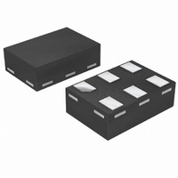
74AUP1G240GF,132 NXP Semiconductors, 74AUP1G240GF,132 Datasheet - Page 7

74AUP1G240GF,132
Manufacturer Part Number
74AUP1G240GF,132
Description
IC INVERTER 1-INPUT 6XSON
Manufacturer
NXP Semiconductors
Series
74AUPr
Datasheet
1.74AUP1G240GM115.pdf
(22 pages)
Specifications of 74AUP1G240GF,132
Package / Case
6-XSON, SOT891
Logic Type
Inverter
Number Of Inputs
1
Number Of Circuits
1
Current - Output High, Low
4mA, 4mA
Voltage - Supply
0.8 V ~ 3.6 V
Operating Temperature
-40°C ~ 125°C
Mounting Type
Surface Mount
Logic Family
AUP
Number Of Channels Per Chip
1
Polarity
Inverting
Supply Voltage (max)
3.6 V
Supply Voltage (min)
0.8 V
Maximum Operating Temperature
+ 125 C
Mounting Style
SMD/SMT
High Level Output Current
- 4 mA
Input Bias Current (max)
0.5 uA
Low Level Output Current
4 mA
Minimum Operating Temperature
- 40 C
Output Type
3-State
Propagation Delay Time
21.6 ns @ 1.1 V to 1.3 V or 12.3 ns @ 1.4 V to 1.6 V or 9.5 ns @ 1.65 V to 1.95 V or 7.1 ns @ 2.3 V to 2.7 V or 6.4 ns @ 3 V to 3.6 V
Number Of Lines (input / Output)
1 / 1
Lead Free Status / RoHS Status
Lead free / RoHS Compliant
Lead Free Status / RoHS Status
Lead free / RoHS Compliant, Lead free / RoHS Compliant
Other names
74AUP1G240GF-H
74AUP1G240GF-H
935281123132
74AUP1G240GF-H
935281123132
NXP Semiconductors
Table 7.
At recommended operating conditions; voltages are referenced to GND (ground = 0 V).
[1]
[2]
74AUP1G240
Product data sheet
Symbol Parameter
V
V
V
I
I
I
ΔI
I
ΔI
I
OZ
OFF
CC
IL
OH
OL
OFF
CC
One input at V
To show I
LOW-level input voltage
HIGH-level output voltage
LOW-level output voltage
input leakage current
OFF-state output current
power-off leakage current
additional power-off
leakage current
supply current
additional supply current
Static characteristics
CC
remains very low when the input-disable feature is enabled.
CC
− 0.6 V, other input at V
…continued
Conditions
V
V
V
V
V
V
V
V
V
V
V
V
V
V
data input; V
V
OE input; V
V
all inputs; V
OE = V
CC
CC
CC
CC
I
I
I
I
CC
I
I
CC
I
CC
CC
CC
CC
I
I
I
I
I
I
I
I
I
I
I
I
I
I
I
I
= V
= V
= GND to 3.6 V; V
= V
or V
or V
= GND or V
O
O
O
O
O
O
O
O
O
O
O
O
O
O
O
O
All information provided in this document is subject to legal disclaimers.
or GND.
= 0.8 V
= 0.9 V to 1.95 V
= 2.3 V to 2.7 V
= 3.0 V to 3.6 V
= 0 V to 3.6 V
= 0 V to 0.2 V
= 0.8 V to 3.6 V
= 3.3 V
= 3.3 V
= −20 μA; V
= −1.1 mA; V
= −1.7 mA; V
= −1.9 mA; V
= −2.3 mA; V
= −3.1 mA; V
= −2.7 mA; V
= −4.0 mA; V
= 20 μA; V
= 1.1 mA; V
= 1.7 mA; V
= 1.9 mA; V
= 2.3 mA; V
= 3.1 mA; V
= 2.7 mA; V
= 4.0 mA; V
IH
IH
IH
O
O
CC
or V
or V
or V
= 0 V to 3.6 V; V
= 0 V to 3.6 V;
Rev. 2 — 13 September 2010
; V
I
I
IL
IL
IL
I
CC
= V
= GND to 3.6 V;
= V
; V
CC
CC
= 0.8 V to 3.6 V
CC
CC
CC
CC
CC
CC
CC
CC
CC
O
; I
CC
CC
CC
CC
CC
CC
CC
CC
= 0.8 V to 3.6 V
= 0 V to 3.6 V;
O
− 0.6 V; I
= 0.8 V to 3.6 V
= 1.1 V
= 1.4 V
= 1.65 V
= 2.3 V
= 2.3 V
= 3.0 V
= 3.0 V
− 0.6 V; I
CC
= 0 A;
= 1.1 V
= 1.4 V
= 1.65 V
= 2.3 V
= 2.3 V
= 3.0 V
= 3.0 V
= 0 V to 3.6 V
CC
= 0 V
O
O
= 0 A;
Low-power inverting buffer/line driver; 3-state
= 0 A;
[1]
[1]
[2]
Min
-
V
-
-
-
-
-
-
-
-
-
-
-
-
-
-
-
-
-
-
0.6 × V
0.93
1.17
1.77
1.67
2.40
2.30
-
CC
− 0.11 -
CC
74AUP1G240
Typ
-
-
-
-
-
-
-
-
-
-
-
-
-
-
-
-
-
-
-
-
-
-
-
-
-
-
-
© NXP B.V. 2010. All rights reserved.
Max
0.25 × V
-
-
-
-
-
-
-
-
0.11
0.33 × V
0.41
0.39
0.36
0.50
0.36
0.50
±0.75
±0.75
±0.75
±0.75
1.4
75
180
1
0.30 × V
0.7
0.9
CC
CC
CC
7 of 22
V
V
V
V
V
V
Unit
V
V
V
V
V
V
V
V
V
V
V
V
V
V
μA
μA
μA
μA
μA
μA
μA
μA


