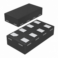
74AUP2G132GT,115 NXP Semiconductors, 74AUP2G132GT,115 Datasheet - Page 7

74AUP2G132GT,115
Manufacturer Part Number
74AUP2G132GT,115
Description
IC NAND SCHMITT DUAL 8-XSON
Manufacturer
NXP Semiconductors
Series
74AUPr
Datasheet
1.74AUP2G132GM125.pdf
(23 pages)
Specifications of 74AUP2G132GT,115
Number Of Circuits
2
Package / Case
8-XSON
Logic Type
NAND Gate - Schmitt Trigger
Number Of Inputs
2
Current - Output High, Low
4mA, 4mA
Voltage - Supply
0.8 V ~ 3.6 V
Operating Temperature
-40°C ~ 125°C
Mounting Type
Surface Mount
Logic Family
AUP
High Level Output Current
- 4 mA
Low Level Output Current
4 mA
Propagation Delay Time
22.6 ns
Supply Voltage (max)
3.6 V
Supply Voltage (min)
0.8 V
Maximum Operating Temperature
+ 125 C
Mounting Style
SMD/SMT
Minimum Operating Temperature
- 40 C
Lead Free Status / RoHS Status
Lead free / RoHS Compliant
Lead Free Status / RoHS Status
Lead free / RoHS Compliant, Lead free / RoHS Compliant
Other names
74AUP2G132GT-G
74AUP2G132GT-G
935280733115
74AUP2G132GT-G
935280733115
Available stocks
Company
Part Number
Manufacturer
Quantity
Price
Company:
Part Number:
74AUP2G132GT,115
Manufacturer:
NXP Semiconductors
Quantity:
4 000
NXP Semiconductors
Table 7.
At recommended operating conditions; voltages are referenced to GND (ground = 0 V).
[1]
12. Dynamic characteristics
Table 8.
Voltages are referenced to GND (ground = 0 V; for test circuit see
74AUP2G132
Product data sheet
Symbol Parameter
ΔI
I
ΔI
Symbol Parameter
C
t
C
t
C
t
CC
pd
pd
pd
L
L
L
OFF
CC
= 5 pF
= 10 pF
= 15 pF
One input at V
additional power-off
leakage current
supply current
additional supply current
propagation delay nA or nB to nY; see
propagation delay nA or nB to nY; see
propagation delay nA or nB to nY; see
Static characteristics
Dynamic characteristics
CC
− 0.6 V, other input at V
Conditions
V
V
V
V
V
V
V
V
V
V
V
V
V
V
V
V
V
V
CC
CC
CC
CC
CC
CC
CC
CC
CC
CC
CC
CC
CC
CC
CC
CC
CC
CC
…continued
= 0.8 V
= 1.1 V to 1.3 V
= 1.4 V to 1.6 V
= 1.65 V to 1.95 V
= 2.3 V to 2.7 V
= 3.0 V to 3.6 V
= 0.8 V
= 1.1 V to 1.3 V
= 1.4 V to 1.6 V
= 1.65 V to 1.95 V
= 2.3 V to 2.7 V
= 3.0 V to 3.6 V
= 0.8 V
= 1.1 V to 1.3 V
= 1.4 V to 1.6 V
= 1.65 V to 1.95 V
= 2.3 V to 2.7 V
= 3.0 V to 3.6 V
Conditions
V
V
V
V
V
V
I
CC
I
CC
I
CC
CC
or V
= GND or V
= V
All information provided in this document is subject to legal disclaimers.
or GND.
= 0 V to 0.2 V
= 0.8 V to 3.6 V
= 3.3 V
CC
O
= 0 V to 3.6 V;
− 0.6 V; I
Rev. 4 — 4 November 2010
Figure 8
Figure 8
Figure 8
CC
; I
O
O
= 0 A;
= 0 A;
[2]
[2]
[2]
Figure
Min
2.6
2.2
1.9
1.7
1.6
3.0
2.5
2.3
2.1
2.0
3.3
2.8
2.6
2.3
2.2
-
-
-
Low-power dual 2-input NAND Schmitt trigger
T
amb
9.
Typ
22.5
26.1
29.6
6.3
4.6
3.9
3.2
2.9
7.2
5.2
4.5
3.8
3.5
8.0
5.8
5.0
4.2
3.9
=
25 °C
[1]
[1]
Min
-
-
-
Max
13.4
15.4
17.2
10.4
8.2
6.6
5.3
4.7
9.3
7.5
6.1
5.5
8.3
6.7
6.1
-
-
-
T
Min
amb
2.4
1.9
1.7
1.5
1.4
2.7
2.2
2.0
1.8
1.8
3.0
2.5
2.3
2.1
2.0
-
-
-
74AUP2G132
=
Typ
-
-
-
−40 °C to +125 °C Unit
(85 °C)
Max
15.1
17.3
11.0
19.4
12.3
10.0
9.7
7.9
6.2
5.6
9.0
7.2
6.5
7.9
7.3
-
-
-
© NXP B.V. 2010. All rights reserved.
Max
±0.75
1.4
75
(125 °C)
Max
16.6
10.7
19.0
12.1
21.3
13.5
11.0
8.7
6.8
6.2
9.9
7.9
7.2
8.7
8.0
-
-
-
ns
ns
ns
ns
ns
ns
ns
ns
ns
ns
ns
ns
ns
ns
ns
ns
ns
ns
7 of 23
Unit
μA
μA
μA


