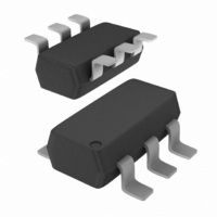
74LVC2G06GV,125 NXP Semiconductors, 74LVC2G06GV,125 Datasheet - Page 3

74LVC2G06GV,125
Manufacturer Part Number
74LVC2G06GV,125
Description
IC INVERTER O-D OUTPUT SC74-6
Manufacturer
NXP Semiconductors
Series
74LVCr
Datasheet
1.74LVC2G06GV125.pdf
(18 pages)
Specifications of 74LVC2G06GV,125
Package / Case
SC-74-6
Logic Type
Inverter with Open Drain
Number Of Inputs
1
Number Of Circuits
2
Current - Output High, Low
32mA, 32mA
Voltage - Supply
1.65 V ~ 5.5 V
Operating Temperature
-40°C ~ 125°C
Mounting Type
Surface Mount
Logic Family
74LVC
Number Of Channels Per Chip
2
Polarity
Inverting
Supply Voltage (max)
5.5 V
Supply Voltage (min)
1.65 V
Maximum Operating Temperature
125 C
Mounting Style
SMD/SMT
Input Bias Current (max)
40 uA
Low Level Output Current
32 mA
Minimum Operating Temperature
-40 C
Output Type
Open Drain
Propagation Delay Time
8.2 ns
Number Of Lines (input / Output)
2 / 2
Lead Free Status / RoHS Status
Lead free / RoHS Compliant
Lead Free Status / RoHS Status
Lead free / RoHS Compliant, Lead free / RoHS Compliant
Other names
74LVC2G06GV-G
74LVC2G06GV-G
935273881125
74LVC2G06GV-G
935273881125
NXP Semiconductors
6. Pinning information
Table 3.
7. Functional description
Table 4.
[1]
8. Limiting values
Table 5.
In accordance with the Absolute Maximum Rating System (IEC 60134). Voltages are referenced to GND (ground = 0 V).
74LVC2G06
Product data sheet
Symbol
1A
GND
2A
2Y
V
1Y
Input nA
L
H
Symbol
V
I
V
IK
Fig 4.
CC
CC
I
H = HIGH voltage level; L = LOW voltage level; Z = high-impedance OFF-state.
GND
1A
2A
and SOT457
Pin configuration SOT363
Pin description
Function table
Limiting values
1
2
3
74LVC2G06
Parameter
supply voltage
input clamping current
input voltage
6.1 Pinning
6.2 Pin description
001aab668
[1]
6
5
4
Pin
1
2
3
4
5
6
1Y
V
2Y
CC
All information provided in this document is subject to legal disclaimers.
Fig 5.
Conditions
V
I
Rev. 4 — 28 October 2010
< 0 V
GND
Description
data input
ground (0 V)
data input
data output
supply voltage
data output
Pin configuration SOT886
1A
2A
Transparent top view
74LVC2G06
1
2
3
Output nY
Z
L
001aab669
6
5
4
1Y
V
2Y
CC
Fig 6.
Inverters with open-drain outputs
[1]
Min
−0.5
−50
−0.5
GND
Pin configuration SOT891,
SOT1115 and SOT1202
1A
2A
Transparent top view
74LVC2G06
74LVC2G06
1
2
3
Max
+6.5
-
+6.5
© NXP B.V. 2010. All rights reserved.
001aag400
6
5
4
1Y
V
2Y
CC
Unit
V
mA
V
3 of 18


