74HCT32DR2G ON Semiconductor, 74HCT32DR2G Datasheet - Page 3
74HCT32DR2G
Manufacturer Part Number
74HCT32DR2G
Description
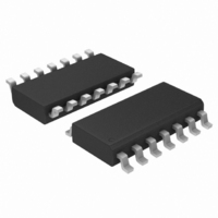
IC GATE OR QUAD 2INPUT 14-SOIC
Manufacturer
ON Semiconductor
Series
74HCTr
Datasheet
1.74HCT32DTR2G.pdf
(8 pages)
Specifications of 74HCT32DR2G
Logic Type
OR Gate
Number Of Inputs
2
Number Of Circuits
4
Current - Output High, Low
4mA, 4mA
Voltage - Supply
4.5 V ~ 5.5 V
Operating Temperature
-55°C ~ 125°C
Mounting Type
Surface Mount
Package / Case
14-SOIC (3.9mm Width), 14-SOL
Lead Free Status / RoHS Status
Lead free / RoHS Compliant
Other names
74HCT32DR2GOSTR


Î Î Î Î Î Î Î Î Î Î Î Î Î Î Î Î Î Î Î Î Î Î Î
Î Î Î Î Î Î Î Î Î Î Î Î Î Î Î Î Î Î Î Î Î Î Î
Stresses exceeding Maximum Ratings may damage the device. Maximum Ratings are stress
ratings only. Functional operation above the Recommended Operating Conditions is not implied.
Extended exposure to stresses above the Recommended Operating Conditions may affect
device reliability.
†Derating — SOIC Package: – 7 mW/_C from 65_ to 125_C
For high frequency or heavy load considerations, see Chapter 2 of the ON Semiconductor High−Speed CMOS Data Book (DL129/D).
MAXIMUM RATINGS
RECOMMENDED OPERATING CONDITIONS
Symbol
Symbol
V
in
V
V
V
T
t
I
I
V
P
T
T
, V
r
I
out
CC
CC
out
stg
CC
, t
in
in
A
D
L
f
out
DC Supply Voltage (Referenced to GND)
DC Input Voltage (Referenced to GND)
DC Output Voltage (Referenced to GND)
DC Input Current, per Pin
DC Output Current, per Pin
DC Supply Current, V
Power Dissipation in Still Air,
Storage Temperature
Lead Temperature, 1 mm from Case for 10 Seconds
DC Supply Voltage (Referenced to GND)
DC Input Voltage, Output Voltage (Referenced to
GND)
Operating Temperature, All Package Types
Input Rise and Fall Time
(Figure 1)
TSSOP Package: − 6.1 mW/_C from 65_ to 125_C
Parameter
Parameter
CC
and GND Pins
SOIC or TSSOP Package
TSSOP Package†
SOIC Package†
V
V
V
CC
CC
CC
= 2.0 V
= 4.5 V
= 6.0 V
http://onsemi.com
– 0.5 to V
– 0.5 to V
3
– 55
Min
4.5
– 0.5 to + 7.0
– 65 to + 150
0
0
0
0
Value
±20
±25
±50
500
450
260
CC
CC
+ 125
1000
Max
V
500
400
5.5
+ 0.5
+ 0.5
CC
Unit
Unit
mW
mA
mA
mA
_C
_C
_C
ns
V
V
V
V
V
circuitry to guard against damage
due to high static voltages or electric
fields. However, precautions must
be taken to avoid applications of any
voltage higher than maximum rated
voltages to this high−impedance cir-
cuit. For proper operation, V
V
range GND v (V
tied to an appropriate logic voltage
level (e.g., either GND or V
Unused outputs must be left open.
out
This device contains protection
Unused inputs must always be
should be constrained to the
in
or V
out
) v V
in
CC
CC
and
).
.
Related parts for 74HCT32DR2G
Image
Part Number
Description
Manufacturer
Datasheet
Request
R


Part Number:
Description:
Quad 2-input NAND Schmitt Trigger
Manufacturer:
Philips Semiconductors (Acquired by NXP)
Datasheet:
Part Number:
Description:
3-to-8 Line Decoder/demultiplexer With Address Latches; Inverting
Manufacturer:
Philips Semiconductors (Acquired by NXP)
Datasheet:
Part Number:
Description:
Dual 2-to-4 Line Decoder/demultiplexer
Manufacturer:
Philips Semiconductors (Acquired by NXP)
Datasheet:
Part Number:
Description:
10-to-4 Line Priority Encoder
Manufacturer:
Philips Semiconductors (Acquired by NXP)
Datasheet:
Part Number:
Description:
8-input Multiplexer
Manufacturer:
Philips Semiconductors (Acquired by NXP)
Datasheet:
Part Number:
Description:
4-to-16 Line Decoder/demultiplexer
Manufacturer:
Philips Semiconductors (Acquired by NXP)
Datasheet:
Part Number:
Description:
Presettable Synchronous 4-bit Binary Counter; Asynchronous Reset
Manufacturer:
Philips Semiconductors (Acquired by NXP)
Datasheet:

Part Number:
Description:
IC BUFF/DVR TRI-ST DUAL 20SOIC
Manufacturer:
Fairchild Semiconductor
Datasheet:

Part Number:
Description:
IC BUFF TRI-ST QD N-INV 14SOIC
Manufacturer:
Fairchild Semiconductor
Datasheet:
Part Number:
Description:
IC BUFF/DVR TRI-ST DUAL 20SOIC
Manufacturer:
Fairchild Semiconductor
Datasheet:
Part Number:
Description:
IC BUFF/DVR TRI-ST 8BIT 20SOIC
Manufacturer:
Fairchild Semiconductor
Datasheet:

Part Number:
Description:
IC BUFF/DVR TRI-ST DUAL 20DIP
Manufacturer:
Fairchild Semiconductor
Datasheet:
Part Number:
Description:
IC TRANSCEIVER TRI-ST 8BIT 20DIP
Manufacturer:
Fairchild Semiconductor
Datasheet:
Part Number:
Description:
IC BUFF/DVR TRI-ST 8BIT 20DIP
Manufacturer:
Fairchild Semiconductor
Datasheet: