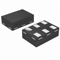
74LVC1G11GM,115 NXP Semiconductors, 74LVC1G11GM,115 Datasheet - Page 4

74LVC1G11GM,115
Manufacturer Part Number
74LVC1G11GM,115
Description
IC SINGLE 3-IN AND GATE 6-XSON
Manufacturer
NXP Semiconductors
Series
74LVCr
Datasheet
1.74LVC1G11GM115.pdf
(17 pages)
Specifications of 74LVC1G11GM,115
Number Of Circuits
1
Package / Case
6-XSON (Micropak™), SOT-886
Logic Type
AND Gate
Number Of Inputs
3
Current - Output High, Low
32mA, 32mA
Voltage - Supply
1.65 V ~ 5.5 V
Operating Temperature
-40°C ~ 125°C
Mounting Type
Surface Mount
Product
AND
Logic Family
74LVC
High Level Output Current
- 32 mA
Low Level Output Current
32 mA
Propagation Delay Time
3 ns
Supply Voltage (max)
5.5 V
Supply Voltage (min)
1.65 V
Maximum Operating Temperature
+ 125 C
Mounting Style
SMD/SMT
Minimum Operating Temperature
- 40 C
Operating Temperature Range
- 40 C to + 125 C
Output Current
50 mA
Output Voltage
5.5 V
Power Dissipation
250 mW
Lead Free Status / RoHS Status
Lead free / RoHS Compliant
Lead Free Status / RoHS Status
Lead free / RoHS Compliant, Lead free / RoHS Compliant
Other names
568-3004-2
935279532115
935279532115
NXP Semiconductors
8. Limiting values
Table 5.
In accordance with the Absolute Maximum Rating System (IEC 60134). Voltages are referenced to GND (ground = 0 V).
[1]
[2]
[3]
9. Recommended operating conditions
Table 6.
74LVC1G11
Product data sheet
Symbol
V
I
V
I
V
I
I
I
P
T
Symbol
V
V
V
T
Δt/ΔV
IK
OK
O
CC
GND
stg
amb
CC
I
O
tot
CC
I
O
The input and output voltage ratings may be exceeded if the input and output current ratings are observed.
When V
For SC-88 and SC-74 packages: above 87.5 °C the value of P
For XSON6 package: above 118 °C the value of P
CC
Limiting values
Recommended operating conditions
Parameter
supply voltage
input clamping current
input voltage
output clamping current
output voltage
output current
supply current
ground current
total power dissipation
storage temperature
= 0 V (Power-down mode), the output voltage can be 5.5 V in normal operation.
Parameter
supply voltage
input voltage
output voltage
ambient temperature
input transition rise and fall rate
All information provided in this document is subject to legal disclaimers.
V
V
Active mode
V
Conditions
Power-down mode
T
amb
I
O
O
tot
< 0 V
Active mode
Conditions
Power-down mode; V
V
V
> V
= 0 V to V
CC
CC
derates linearly with 7.8 mW/K.
Rev. 5 — 30 July 2010
= −40 °C to +125 °C
CC
= 1.65 V to 2.7 V
= 2.7 V to 5.5 V
or V
tot
CC
O
derates linearly with 4.0 mW/K.
< 0 V
CC
= 0 V
[1][2]
[1][2]
[1]
[3]
Min
1.65
0
0
0
−40
-
-
Min
−0.5
−50
−0.5
-
−0.5
−0.5
-
-
−100
-
−65
Single 3-input AND gate
Typ
-
-
-
-
-
-
-
74LVC1G11
Max
+6.5
-
+6.5
±50
V
+6.5
±50
100
-
250
+150
CC
© NXP B.V. 2010. All rights reserved.
Max
5.5
5.5
V
5.5
+125
20
10
+ 0.5
CC
Unit
V
V
V
V
°C
ns/V
ns/V
Unit
V
mA
V
mA
V
V
mA
mA
mA
mW
°C
4 of 17


