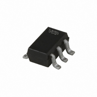
74LVC2GU04GW,125 NXP Semiconductors, 74LVC2GU04GW,125 Datasheet - Page 9

74LVC2GU04GW,125
Manufacturer Part Number
74LVC2GU04GW,125
Description
IC DUAL INVERTER SC88-6
Manufacturer
NXP Semiconductors
Series
74LVCr
Datasheet
1.74LVC2GU04GW125.pdf
(19 pages)
Specifications of 74LVC2GU04GW,125
Number Of Circuits
2
Logic Type
Inverter
Package / Case
SC-70-6, SC-88, SOT-363
Number Of Inputs
1
Current - Output High, Low
32mA, 32mA
Voltage - Supply
1.65 V ~ 5.5 V
Operating Temperature
-40°C ~ 125°C
Mounting Type
Surface Mount
Logic Family
74LVC
High Level Output Current
- 32 mA
Low Level Output Current
32 mA
Propagation Delay Time
5.6 ns
Supply Voltage (max)
5.5 V
Supply Voltage (min)
1.65 V
Maximum Operating Temperature
+ 125 C
Minimum Operating Temperature
- 40 C
Mounting Style
SMD/SMT
Operating Supply Voltage
2.7 V
Lead Free Status / RoHS Status
Lead free / RoHS Compliant
Lead Free Status / RoHS Status
Lead free / RoHS Compliant, Lead free / RoHS Compliant
Other names
568-4843-2
74LVC2GU04GW,125
74LVC2GU04GW-G
74LVC2GU04GW-G
935274026125
74LVC2GU04GW,125
74LVC2GU04GW-G
74LVC2GU04GW-G
935274026125
Available stocks
Company
Part Number
Manufacturer
Quantity
Price
Company:
Part Number:
74LVC2GU04GW,125
Manufacturer:
NXP Semiconductors
Quantity:
61
NXP Semiconductors
13. Application information
74LVC2GU04
Product data sheet
Fig 11. Linear amplifier configuration
V
G
A
R1 ≥ 3 kΩ, R2 ≤ 1 MΩ.
Z
Typical unity gain bandwidth product is 5 MHz.
A
L
o(p-p)
u
OL
u
> 10 kΩ; A
= voltage amplification.
=
= open loop gain.
1 μF
= V
–
----------------------------------------- -
1
CC
+
R1
------ - 1
R2
R1
− 1.5 V centered at 0.5V
OL
G
(
Some applications are:
Remark: All values given are typical unless otherwise specified.
= 20 (typical).
OL
•
•
+
G
Linear amplifier (see
In crystal oscillator design (see
OL
U04
V
)
R2
CC
All information provided in this document is subject to legal disclaimers.
mna052
CC
.
Z L
Rev. 6 — 27 October 2010
Figure
11)
Fig 12. Crystal oscillator configuration
Figure
12)
C1 = 47 pF (typical).
C2 = 22 pF (typical).
R1 = 1 MΩ to 10 MΩ (typical).
R2 optimum value depends on the frequency and
required stability against changes in V
minimum I
f = 10 MHz).
U04
R1
CC
(I
CC
is typically 2 mA at V
out
74LVC2GU04
R2
C1
© NXP B.V. 2010. All rights reserved.
mna053
CC
CC
C2
Dual inverter
or average
= 3.3 V and
9 of 19


