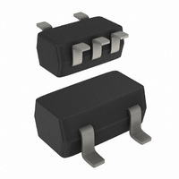
74LVC1G00GW,125 NXP Semiconductors, 74LVC1G00GW,125 Datasheet - Page 2

74LVC1G00GW,125
Manufacturer Part Number
74LVC1G00GW,125
Description
IC SNGL 2-IN NAND GATE 5TSSOP
Manufacturer
NXP Semiconductors
Series
74LVCr
Datasheet
1.74LVC1G00GW125.pdf
(17 pages)
Specifications of 74LVC1G00GW,125
Number Of Circuits
1
Package / Case
SC-70-5, SC-88A, SOT-323-5, SOT-353, 5-TSSOP
Logic Type
NAND Gate
Number Of Inputs
2
Current - Output High, Low
32mA, 32mA
Voltage - Supply
1.65 V ~ 5.5 V
Operating Temperature
-40°C ~ 125°C
Mounting Type
Surface Mount
Product
NAND
Logic Family
LVC
High Level Output Current
- 32 mA
Low Level Output Current
32 mA
Propagation Delay Time
2.2 ns
Supply Voltage (max)
5.5 V
Supply Voltage (min)
1.65 V
Maximum Operating Temperature
+ 125 C
Mounting Style
SMD/SMT
Minimum Operating Temperature
- 40 C
Lead Free Status / RoHS Status
Lead free / RoHS Compliant
Lead Free Status / RoHS Status
Lead free / RoHS Compliant, Lead free / RoHS Compliant
Other names
568-4609-2
74LVC1G00GW-G
74LVC1G00GW-G
935268378125
74LVC1G00GW-G
74LVC1G00GW-G
935268378125
Available stocks
Company
Part Number
Manufacturer
Quantity
Price
Part Number:
74LVC1G00GW,125
Manufacturer:
NXP/恩智浦
Quantity:
20 000
NXP Semiconductors
3. Ordering information
Table 1.
4. Marking
Table 2.
[1]
5. Functional diagram
74LVC1G00
Product data sheet
Type number
74LVC1G00GW
74LVC1G00GV
74LVC1G00GM
74LVC1G00GF
74LVC1G00GN
74LVC1G00GS
Type number
74LVC1G00GW
74LVC1G00GV
74LVC1G00GM
74LVC1G00GF
74LVC1G00GN
74LVC1G00GS
Fig 1.
The pin 1 indicator is located on the lower left corner of the device, below the marking code.
1
2
Logic symbol
Ordering information
Marking codes
B
A
mna097
Package
Temperature range
−40 °C to +125 °C
−40 °C to +125 °C
−40 °C to +125 °C
−40 °C to +125 °C
−40 °C to +125 °C
−40 °C to +125 °C
Y
4
All information provided in this document is subject to legal disclaimers.
Fig 2.
Name
TSSOP5
SC-74A
XSON6
XSON6
XSON6
XSON6
Rev. 8 — 20 October 2010
1
2
IEC logic symbol
&
Marking
VA
V00
VA
VA
VA
VA
mna098
plastic extremely thin small outline package;
plastic extremely thin small outline package;
extremely thin small outline package; no leads;
extremely thin small outline package; no leads;
Description
plastic thin shrink small outline package;
5 leads; body width 1.25 mm
plastic surface-mounted package; 5 leads
no leads; 6 terminals; body 1 × 1.45 × 0.5 mm
no leads; 6 terminals; body 1 × 1 × 0.5 mm
6 terminals; body 0.9 × 1.0 × 0.35 mm
6 terminals; body 1.0 × 1.0 × 0.35 mm
[1]
4
Fig 3.
B
A
Logic diagram
Single 2-input NAND gate
74LVC1G00
© NXP B.V. 2010. All rights reserved.
Version
SOT353-1
SOT753
SOT886
SOT891
SOT1115
SOT1202
mna099
2 of 17
Y


