NBSG53ABA ON Semiconductor, NBSG53ABA Datasheet
NBSG53ABA
Specifications of NBSG53ABA
Available stocks


Related parts for NBSG53ABA

NBSG53ABA Summary of contents
Page 1
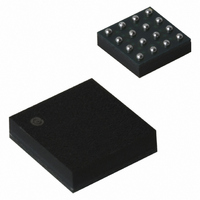
... Application Note AND8002/D ORDERING INFORMATION Device Package Shipping NBSG53ABA 4x4 mm 100 Units/Tray FCBGA-16 NBSG53ABAR2 4x4 mm 500/Tape & Reel FCBGA-16 NBSG53MN 3x3 mm 123 Units/Rail QFN-16 NBSG53MNR2 3x3 mm 3000/Tape & Reel QFN-16 Board Description NBSG53ABAEVB NBSG53ABA Evaluation Board Publication Order Number: NBSG53A/D ...
Page 2
A VTD D D VTD B CLK VTCLK CLK VTCLK SEL OLS CC D Figure 1. BGA-16 Pinout (Top View) Table 1. Pin Description Pin BGA QFN Name C2 1 ...
Page 3
V CC OLS VTD VTD VTCLK 50 W CLK CLK 50 W VTCLK R SEL Table 2. OUTPUT LEVEL SELECT (OLS) OLS Q/Q VPP OLS Sensitivity V 800 mV CC ...
Page 4
Table 5. ATTRIBUTES Positive Operating Voltage Range for V Negative Operating Voltage Range for V Internal Input Pulldown Resistor (R, SEL) ESD Protection Moisture Sensitivity (Note 5) Flammability Rating Oxygen Index Transistor Count Meets or exceeds JEDEC Spec EIA/JESD78 IC ...
Page 5
Table 7. DC CHARACTERISTICS, INPUT WITH PECL OUTPUT Symbol Characteristic I Negative Power Supply Current EE V Output HIGH Voltage (Note 10 Output LOW Voltage (Note 10) OL (OLS = V (OLS = V CC (OLS = V ...
Page 6
Table 8. DC CHARACTERISTICS, INPUT WITH PECL OUTPUT Symbol Characteristic I Negative Power Supply Current EE V Output HIGH Voltage (Note 16 Output LOW Voltage (Note 16) OL (OLS = V (OLS = ...
Page 7
Table 9. DC CHARACTERISTICS, NECL INPUT WITH NECL OUTPUT -3.465 V to -2.375 V (Note 21 Symbol Characteristic I Negative Power Supply Current EE V Output HIGH Voltage (Note 22 ...
Page 8
Table 9. DC CHARACTERISTICS, NECL INPUT WITH NECL OUTPUT -3.465 V to -2.375 V (Note 21) (continued Symbol Symbol Characteristic Characteristic R Internal Input Termination Resistor TIN I Input HIGH Current (@V ...
Page 9
Table 10. AC CHARACTERISTICS for FCBGA- -3.465 V to -2.375 Symbol Characteristic f Maximum Frequency max (See Figures 10, and 11) (See Figures ...
Page 10
Table 11. AC CHARACTERISTICS for QFN- -3.465 V to -2.375 Symbol Characteristic f Maximum Frequency max (See Figures 10, and 11) (See Figures ...
Page 11
OLS = V 800 700 OLS = V 600 *OLS = V 500 400 OLS = V 300 200 100 Figure 4. Output Voltage Amplitude (V Input Frequency (f ) for DFF Mode (V in 900 ...
Page 12
OLS = V 800 700 OLS = V 600 500 *OLS = V 400 OLS = V 300 200 100 Figure 6. Output Voltage Amplitude (V Input Frequency (f ) for DFF Mode (V in 900 ...
Page 13
NBSG53A 1200 V (Q) OH 1100 1000 900 V (Q) OH 800 700 600 V (Q) OL 500 400 300 V 200 100 INPUT FREQUENCY (GHz) Figure (Q/Q) vs. ...
Page 14
NBSG53A 100 DIV/2 Mode DFF Mode INPUT FREQUENCY (GHz) Figure 10. Duty Cycle % vs. Input Frequency ( 3.3 ...
Page 15
NBSG53A 300 200 100 0 -100 -200 -300 -400 -500 -600 -700 400 V - 800 (mV) OLS Figure 12. Typical OLS Input Current vs. OLS Input Voltage ( 3.3 ...
Page 16
NBSG53A CLK CLK PLH Figure 14. AC Reference Measurement Q Driver Device 2.0 V Figure 15. Typical Termination for Output Driver and Device Evaluation (Refer to ...
Page 17
PLASTIC (mm) BGA FLIP CHIP PACKAGE LASER MARK FOR PIN 1 IDENTIFICATION IN -X- THIS AREA D - VIEW M DETAIL K _ ...
Page 18
... PLANE JAPAN: ON Semiconductor, Japan Customer Focus Center 2-9-1 Kamimeguro, Meguro-ku, Tokyo, Japan 153-0051 Phone: 81-3-5773-3850 ON Semiconductor Website: http://onsemi.com For additional information, please contact your local Sales Representative. http://onsemi.com 18 NOTES: 1. DIMENSIONING AND TOLERANCING PER ANSI Y14.5M, 1982. 2. CONTROLLING DIMENSION: MILLIMETERS. ...