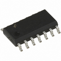
74LVQ74SCX Fairchild Semiconductor, 74LVQ74SCX Datasheet - Page 3

74LVQ74SCX
Manufacturer Part Number
74LVQ74SCX
Description
IC FLIP FLOP DUAL D POS 14SOIC
Manufacturer
Fairchild Semiconductor
Series
74LVQr
Type
D-Typer
Datasheet
1.74LVQ74SJX.pdf
(6 pages)
Specifications of 74LVQ74SCX
Function
Set(Preset) and Reset
Output Type
Differential
Number Of Elements
2
Number Of Bits Per Element
1
Frequency - Clock
125MHz
Delay Time - Propagation
8ns
Trigger Type
Positive Edge
Current - Output High, Low
12mA, 12mA
Voltage - Supply
2 V ~ 3.6 V
Operating Temperature
-40°C ~ 85°C
Mounting Type
Surface Mount
Package / Case
14-SOIC (3.9mm Width), 14-SOL
Lead Free Status / RoHS Status
Lead free / RoHS Compliant
V
V
V
V
I
I
I
I
V
V
V
V
Absolute Maximum Ratings
DC Electrical Characteristics
IN
OLD
OHD
CC
Note 3: All outputs loaded; thresholds on input associated with output under test.
Note 4: Maximum test duration 2.0 ms, one output loaded at a time.
Note 5: Incident wave switching on transmission lines with impedances as low as 75
Note 6: Worst case package.
Note 7: Max number of outputs defined as (n). Data inputs are driven 0V to 3.3V; one output at GND.
Note 8: Max number of Data Inputs (n) switching. (n
(V
IH
IL
OH
OL
OLP
OLV
IHD
ILD
Supply Voltage (V
DC Input Diode Current (I
DC Input Voltage (V
DC Output Diode Current (I
DC Output Voltage (V
DC Output Source
DC V
Storage Temperature (T
DC Latch-Up Source or
Symbol
IHD
V
V
V
V
or Sink Current (I
(I
Sink Current
), f
CC
I
I
O
O
CC
V
or I
1 MHz.
V
0.5V
CC
or Ground Current
0.5V
CC
Minimum High Level
Maximum Low Level
Input Voltage
Minimum High Level
Output Voltage
Maximum Low Level
Output Voltage
Maximum Input
Leakage Current
Minimum Dynamic
Output Current (Note 4)
Maximum Quiescent
Supply Current
Quiet Output
Maximum Dynamic V
Quiet Output
Minimum Dynamic V
Maximum High Level
Dynamic Input Voltage
Maximum Low Level
Dynamic Input Voltage
GND
0.5V
)
0.5V
CC
Parameter
O
I
)
)
)
O
)
STG
IK
)
OK
OL
)
OL
)
V
0.5V to V
0.5V to V
3.0
3.0
3.0
3.0
3.0
3.0
3.6
3.6
3.6
3.6
3.3
3.3
3.3
3.3
(V)
CC
65 C to 150 C
1) inputs switching 0V to 3.3V. Input-under-test switching: 3.3V to threshold (V
0.5V to 7.0V
(Note 1)
0.002
CC
CC
2.99
Typ
1.5
1.5
0.2
1.7
1.6
0.2
200 mA
100 mA
T
20 mA
20 mA
20 mA
20 mA
50 mA
A
0.5V
0.5V
25 C
2.58
0.36
3
2.0
0.8
2.9
0.1
2.0
0.8
2.0
0.8
0.1
0.8
Recommended Operating
Conditions
Note 1: The “Absolute Maximum Ratings” are those values beyond which
the safety of the device cannot be guaranteed. The device should not be
operated at these limits. The parametric values defined in the Electrical
Characteristics tables are not guaranteed at the absolute maximum ratings.
The “Recommended Operating Conditions” table will define the conditions
for actual device operation.
Note 2: Unused inputs must be held HIGH or LOW. They may not float.
Supply Voltage (V
Input Voltage (V
Output Voltage (V
Operating Temperature (T
Minimum Input Edge Rate ( V/ t)
Guaranteed Limits
V
V
IN
CC
for commercial temperature range is guaranteed for 74LVQ.
from 0.8V to 2.0V
T
@ 3.0V
A
40 C to 85 C
2.48
0.44
20.0
2.0
0.8
2.9
0.1
36
1.0
25
I
)
CC
O
(Note 2)
)
)
A
)
Units
mA
mA
V
V
V
V
V
V
V
V
V
V
A
A
V
or V
V
or V
I
V
I
I
V
I
V
GND
V
V
V
or GND
(Note 6)(Note 7)
(Note 6)(Note 7)
(Note 6)(Note 8)
(Note 6)(Note 8)
OUT
OH
OUT
OL
www.fairchildsemi.com
OUT
OUT
IN
IN
I
OLD
OHD
IN
CC
CC
V
ILD
12 mA
V
V
V
CC
50 A
12 mA
Conditions
IL
IL
CC
40 C to 85 C
), 0V to threshold
0.1V
0.1V
0.8V Max (Note 5)
2.0V Min (Note 5)
50 A
,
0.1V
0.1V
or V
or V
2.0V to 3.6V
125 mV/ns
0V to V
0V to V
IH
IH
(Note 3)
(Note 3)
CC
CC


