MC74HCT273ADWG ON Semiconductor, MC74HCT273ADWG Datasheet - Page 4
MC74HCT273ADWG
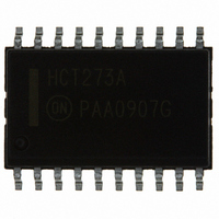
Manufacturer Part Number
MC74HCT273ADWG
Description
IC FLIP FLOP OCTAL D 20-SOIC
Manufacturer
ON Semiconductor
Series
74HCTr
Type
D-Type Busr
Datasheet
1.MC74HCT273ADTR2G.pdf
(8 pages)
Specifications of MC74HCT273ADWG
Function
Reset
Output Type
Non-Inverted
Number Of Elements
1
Number Of Bits Per Element
8
Frequency - Clock
30MHz
Delay Time - Propagation
25ns
Trigger Type
Positive Edge
Current - Output High, Low
4mA, 4mA
Voltage - Supply
4.5 V ~ 5.5 V
Operating Temperature
-55°C ~ 125°C
Mounting Type
Surface Mount
Package / Case
20-SOIC (7.5mm Width)
Logic Family
HCT
Technology
CMOS
Number Of Bits
8
Number Of Elements
1
Clock-edge Trigger Type
Positive-Edge
Polarity
Non-Inverting
Operating Supply Voltage (typ)
5V
Package Type
SOIC W
Propagation Delay Time
35ns
Low Level Output Current
4mA
High Level Output Current
-4mA
Operating Supply Voltage (min)
4.5V
Operating Supply Voltage (max)
5.5V
Operating Temp Range
-55C to 125C
Operating Temperature Classification
Military
Mounting
Surface Mount
Pin Count
20
Number Of Circuits
8
Logic Type
D-Type Flip-Flop
Input Type
Single-Ended
Supply Voltage (max)
5.5 V
Maximum Operating Temperature
+ 125 C
Mounting Style
SMD/SMT
Minimum Operating Temperature
- 55 C
Supply Voltage (min)
4.5 V
Lead Free Status / RoHS Status
Lead free / RoHS Compliant
Other names
MC74HCT273ADWG
MC74HCT273ADWGOS
MC74HCT273ADWGOS


Î Î Î Î Î Î Î Î Î Î Î Î Î Î Î Î Î Î Î Î Î Î Î Î Î Î Î Î Î Î Î Î Î
Î Î Î Î Î Î Î Î Î Î Î Î Î Î Î Î Î Î Î Î Î Î Î Î Î Î Î Î Î Î Î Î Î
Î Î Î Î
Î Î Î Î
Î Î Î Î
Î Î Î Î
Î Î Î Î
Î Î Î Î
Î Î Î Î
Î Î Î Î
Î Î Î Î
Î Î Î Î
Î Î Î Î
Î Î Î Î
Î Î Î Î
Î Î Î Î
Î Î Î Î
Î Î Î Î
TIMING REQUIREMENTS
Symbol
t
t
t
r
rec
t
t
t
su
, t
w
w
h
f
Î Î Î Î Î Î Î Î Î Î Î Î Î Î Î
Î Î Î Î Î Î Î Î Î Î Î Î Î Î Î
Î Î Î Î Î Î Î Î Î Î Î Î Î Î Î
Î Î Î Î Î Î Î Î Î Î Î Î Î Î Î
Î Î Î Î Î Î Î Î Î Î Î Î Î Î Î
Î Î Î Î Î Î Î Î Î Î Î Î Î Î Î
Î Î Î Î Î Î Î Î Î Î Î Î Î Î Î
Î Î Î Î Î Î Î Î Î Î Î Î Î Î Î
Î Î Î Î Î Î Î Î Î Î Î Î Î Î Î
Î Î Î Î Î Î Î Î Î Î Î Î Î Î Î
Î Î Î Î Î Î Î Î Î Î Î Î Î Î Î
Î Î Î Î Î Î Î Î Î Î Î Î Î Î Î
Î Î Î Î Î Î Î Î Î Î Î Î Î Î Î
Î Î Î Î Î Î Î Î Î Î Î Î Î Î Î
Î Î Î Î Î Î Î Î Î Î Î Î Î Î Î
Î Î Î Î Î Î Î Î Î Î Î Î Î Î Î
Minimum Setup Time, Data to Clock
Minimum Hold Time, Clock to Data
Minimum Recovery Time, Set or Reset Inactive to Clock
Minimum Pulse Width, Clock
Minimum Pulse Width, Set or Reset
Maximum Input Rise and Fall Times
(V
CC
Parameter
= 5.0 V ± 10%, C
L
= 50 pF, Input t
http://onsemi.com
4
Î Î Î
Î Î Î
Î Î Î
Î Î Î
Î Î Î
Î Î Î
Î Î Î
Î Î Î
Î Î Î
Î Î Î
Î Î Î
Î Î Î
Î Î Î
Î Î Î
Î Î Î
Î Î Î
r
= t
Fig.
f
3
3
2
1
2
1
= 6.0 ns)
Î Î Î Î Î Î Î Î Î Î Î Î
Î Î Î Î Î Î Î Î Î Î Î Î
Î Î Î Î Î
Î Î Î Î Î
Î Î Î
Î Î Î
Î Î Î
Î Î Î
Î Î Î
Î Î Î
Î Î Î
Î Î Î
Î Î Î
Î Î Î
Î Î Î
Î Î Î
Î Î Î
Î Î Î
– 55 to 25_C
Min
3.0
5.0
10
12
12
Î Î Î
Î Î Î
Î Î Î
Î Î Î Î Î Î
Î Î Î
Î Î Î
Î Î Î
Î Î Î
Î Î Î
Î Î Î
Î Î Î
Î Î Î Î Î Î
Î Î Î
Î Î Î
Max
500
Guaranteed Limit
Î Î Î Î Î
Î Î Î Î Î
Î Î Î
Î Î Î
Î Î Î
Î Î Î
Î Î Î
Î Î Î
Î Î Î
Î Î Î
Î Î Î
Î Î Î
Î Î Î
Î Î Î
Min
3.0
5.0
12
15
15
v 85_C
Î Î Î
Î Î Î
Î Î Î
Î Î Î Î Î Î Î
Î Î Î
Î Î Î
Î Î Î
Î Î Î
Î Î Î
Î Î Î
Î Î Î
Î Î Î Î Î Î Î
Î Î Î
Î Î Î
Max
500
Î Î Î Î
Î Î Î Î
Î Î
Î Î
Î Î
Î Î
Î Î
Î Î
Î Î
Î Î
Î Î
Î Î
Min
3.0
5.0
15
18
18
v 125_C
Î Î Î
Î Î Î
Î Î Î
Î Î Î Î Î Î
Î Î Î
Î Î Î
Î Î Î
Î Î Î
Î Î Î
Î Î Î
Î Î Î
Î Î Î Î Î Î
Î Î Î
Î Î Î
Max
500
Î Î Î
Î Î Î
Î Î Î
Î Î Î
Î Î Î
Î Î Î
Î Î Î
Î Î Î
Î Î Î
Î Î Î
Î Î Î
Î Î Î
Î Î Î
Î Î Î
Unit
ns
ns
ns
ns
ns
ns
Related parts for MC74HCT273ADWG
Image
Part Number
Description
Manufacturer
Datasheet
Request
R

Part Number:
Description:
ON Semiconductor [VOLTAGE REGULATOR]
Manufacturer:
ON Semiconductor
Datasheet:
Part Number:
Description:
357-036-542-201 CARDEDGE 36POS DL .156 BLK LOPRO
Manufacturer:
ON Semiconductor
Datasheet:
Part Number:
Description:
357-036-542-201 CARDEDGE 36POS DL .156 BLK LOPRO
Manufacturer:
ON Semiconductor
Datasheet:
Part Number:
Description:
357-036-542-201 CARDEDGE 36POS DL .156 BLK LOPRO
Manufacturer:
ON Semiconductor
Datasheet:
Part Number:
Description:
357-036-542-201 CARDEDGE 36POS DL .156 BLK LOPRO
Manufacturer:
ON Semiconductor
Datasheet:
Part Number:
Description:
357-036-542-201 CARDEDGE 36POS DL .156 BLK LOPRO
Manufacturer:
ON Semiconductor
Datasheet:
Part Number:
Description:
357-036-542-201 CARDEDGE 36POS DL .156 BLK LOPRO
Manufacturer:
ON Semiconductor
Datasheet:
Part Number:
Description:
357-036-542-201 CARDEDGE 36POS DL .156 BLK LOPRO
Manufacturer:
ON Semiconductor
Datasheet:
Part Number:
Description:
357-036-542-201 CARDEDGE 36POS DL .156 BLK LOPRO
Manufacturer:
ON Semiconductor
Datasheet:
Part Number:
Description:
357-036-542-201 CARDEDGE 36POS DL .156 BLK LOPRO
Manufacturer:
ON Semiconductor
Datasheet:
Part Number:
Description:
357-036-542-201 CARDEDGE 36POS DL .156 BLK LOPRO
Manufacturer:
ON Semiconductor
Datasheet:
Part Number:
Description:
Manufacturer:
ON Semiconductor
Datasheet:
Part Number:
Description:
Manufacturer:
ON Semiconductor
Datasheet:
Part Number:
Description:
Manufacturer:
ON Semiconductor
Datasheet: