MC74HCT273ADWG ON Semiconductor, MC74HCT273ADWG Datasheet
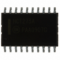
IC FLIP FLOP OCTAL D 20-SOIC

MC74HCT273ADWG

Manufacturer Part Number
MC74HCT273ADWG
Description
IC FLIP FLOP OCTAL D 20-SOIC
Manufacturer
ON Semiconductor
Series
74HCTr
Type
D-Type Busr
Datasheet

Specifications of MC74HCT273ADWG

Function
Reset
Output Type
Non-Inverted
Number Of Elements
1
Number Of Bits Per Element
8
Frequency - Clock
30MHz
Delay Time - Propagation
25ns
Trigger Type
Positive Edge
Current - Output High, Low
4mA, 4mA
Voltage - Supply
4.5 V ~ 5.5 V
Operating Temperature
-55°C ~ 125°C
Mounting Type
Surface Mount
Package / Case
20-SOIC (7.5mm Width)
Logic Family
HCT
Technology
CMOS
Number Of Bits
8
Number Of Elements
1
Clock-edge Trigger Type
Positive-Edge
Polarity
Non-Inverting
Operating Supply Voltage (typ)
5V
Package Type
SOIC W
Propagation Delay Time
35ns
Low Level Output Current
4mA
High Level Output Current
-4mA
Operating Supply Voltage (min)
4.5V
Operating Supply Voltage (max)
5.5V
Operating Temp Range
-55C to 125C
Operating Temperature Classification
Military
Mounting
Surface Mount
Pin Count
20
Number Of Circuits
8
Logic Type
D-Type Flip-Flop
Input Type
Single-Ended
Supply Voltage (max)
5.5 V
Maximum Operating Temperature
+ 125 C
Mounting Style
SMD/SMT
Minimum Operating Temperature
- 55 C
Supply Voltage (min)
4.5 V
Lead Free Status / RoHS Status
Lead free / RoHS Compliant
Other names
MC74HCT273ADWG
MC74HCT273ADWGOS
MC74HCT273A
Octal D Flip−Flop with
Common Clock and Reset
with LSTTL−Compatible
Inputs
High−Performance Silicon−Gate CMOS
interfacing TTL or NMOS outputs to High−Speed CMOS inputs.
Reset inputs. Each flip−flop is loaded with a low−to−high transition of
the Clock input. Reset is asynchronous and active low.
w
© Semiconductor Components Industries, LLC, 2006
March, 2006 − Rev. 10
The MC74HCT273A may be used as a level converter for
The HCT273A is identical in pinout to the LS273.
This device consists of eight D flip−flops with common Clock and
No. 7A
These devices are available in Pb−free package(s). Specifications herein
apply to both standard and Pb−free devices. Please see our website at
www.onsemi.com for specific Pb−free orderable part numbers, or
contact your local ON Semiconductor sales office or representative.
Output Drive Capability: 10 LSTTL Loads
TTL/NMOS Compatible Input Levels
Outputs Directly Interface to CMOS, NMOS and TTL
Operating Voltage Range: 4.5 to 5.5 V
Low Input Current: 1.0 μA
In Compliance with the Requirements Defined by JEDEC Standard
Chip Complexity: 284 FETs or 71 Equivalent Gates
1
20
MC74HCT273AN
MC74HCT273ADW
MC74HCT273ADWR2 SOIC−WIDE
20
1
1
Device
ORDERING INFORMATION
RESET
A
WL = Wafer Lot
YY = Year
WW = Work Week
GND
SOIC WIDE−20
http://onsemi.com
PIN ASSIGNMENT
Q0
Q1
D0
D1
Q2
D2
D3
Q3
DW SUFFIX
CASE 751D
= Assembly Location
CASE 738
N SUFFIX
1
2
3
4
5
6
7
8
9
10
PDIP−20
SOIC−WIDE
Publication Order Number:
Package
PDIP−20
20
19
18
17
16
15
14
13
12
11
MC74HCT273A/D
20
20
MC74HCT273AN
1
1
V
Q7
D7
D6
Q6
Q5
D5
D4
Q4
CLOCK
DIAGRAMS
MARKING
CC
AWLYYWW
AWLYYWW
HCT273A
1000 / Reel
1440 / Box
Shipping
38 / Rail

Related parts for MC74HCT273ADWG

MC74HCT273ADWG Summary of contents

Page 1

... These devices are available in Pb−free package(s). Specifications herein apply to both standard and Pb−free devices. Please see our website at www.onsemi.com for specific Pb−free orderable part numbers, or contact your local ON Semiconductor sales office or representative. © Semiconductor Components Industries, LLC, 2006 March, 2006 − Rev. 10 http://onsemi.com PDIP− ...

Page 2

... Functional operation should be restricted to the Recommended Operating Conditions. †Derating — Plastic DIP: – 10 mW/_C from 65_ to 125_C SOIC Package: – 7 mW/_C from 65_ to 125_C For high frequency or heavy load considerations, see Chapter 2 of the ON Semiconductor High−Speed CMOS Data Book (DL129/D). RECOMMENDED OPERATING CONDITIONS Symbol Parameter Î ...

Page 3

... NOTE: Information on typical parametric values can be found in Chapter 2 of the ON Semiconductor High−Speed CMOS Data Book Î Î Î Î Î Î Î Î Î Î Î Î Î ...

Page 4

TIMING REQUIREMENTS (V = 5.0 V ± ...

Page 5

V CLOCK 1 1/f max t t PLH PHL 90 TLH THL Figure 1. VALID DATA 1 1.3 V ...

Page 6

SEATING PLANE 20X 0. 18X PACKAGE DIMENSIONS PDIP−20 N SUFFIX PLASTIC DIP PACKAGE CASE 738−03 ISSUE ...

Page 7

Notes http://onsemi.com 7 ...

Page 8

... Fax: 480−829−7709 or 800−344−3867 Toll Free USA/Canada Email: orderlit@onsemi.com N. American Technical Support: 800−282−9855 Toll Free USA/Canada Japan: ON Semiconductor, Japan Customer Focus Center 2−9−1 Kamimeguro, Meguro−ku, Tokyo, Japan 153−0051 Phone: 81−3−5773−3850 http://onsemi.com 8 ON Semiconductor Website: http://onsemi ...

Related keywords