MC74VHC74DTG ON Semiconductor, MC74VHC74DTG Datasheet
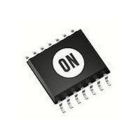
IC FLIP FLOP DUAL D S/R 14-TSSOP

MC74VHC74DTG

Manufacturer Part Number
MC74VHC74DTG
Description
IC FLIP FLOP DUAL D S/R 14-TSSOP
Manufacturer
ON Semiconductor
Series
74VHCr
Type
D-Typer
Datasheet

Specifications of MC74VHC74DTG

Function
Set(Preset) and Reset
Output Type
Differential
Number Of Elements
2
Number Of Bits Per Element
1
Frequency - Clock
170MHz
Delay Time - Propagation
7.3ns
Trigger Type
Positive Edge
Current - Output High, Low
8mA, 8mA
Voltage - Supply
2 V ~ 5.5 V
Operating Temperature
-55°C ~ 125°C
Mounting Type
Surface Mount
Package / Case
14-TSSOP
Number Of Circuits
2
Logic Family
74VHC
Logic Type
D-Type Flip-Flop
Polarity
Inverting/Non-Inverting
Input Type
Single-Ended
Propagation Delay Time
15.4 ns
High Level Output Current
- 8 mA
Low Level Output Current
8 mA
Supply Voltage (max)
5.5 V
Maximum Operating Temperature
+ 85 C
Mounting Style
SMD/SMT
Minimum Operating Temperature
- 40 C
Supply Voltage (min)
2 V
Lead Free Status / RoHS Status
Lead free / RoHS Compliant

Available stocks

Company
Part Number
Manufacturer
Quantity
Price
Part Number:
MC74VHC74DTG
Manufacturer:
ON/安森美
Quantity:
20 000
MC74VHC74
Dual D-Type Flip-Flop
with Set and Reset
flip−flop fabricated with silicon gate CMOS technology. It achieves
high speed operation similar to equivalent Bipolar Schottky TTL
while maintaining CMOS low power dissipation.
during the positive going transition of the Clock pulse.
accomplished by setting the appropriate input Low.
output which provides high noise immunity and stable output. The
inputs tolerate voltages up to 7.0 V, allowing the interface of 5.0 V
systems to 3.0 V systems.
Features
© Semiconductor Components Industries, LLC, 2008
July, 2008 − Rev. 7
RD1
CP1
SD1
The MC74VHC74 is an advanced high speed CMOS D−type
The signal level applied to the D input is transferred to Q output
Reset (RD) and Set (SD) are independent of the Clock (CP) and are
The internal circuit is composed of three stages, including a buffer
High Speed: f
Low Power Dissipation: I
High Noise Immunity: V
Power Down Protection Provided on Inputs
Balanced Propagation Delays
Designed for 2.0 V to 5.5 V Operating Range
Low Noise: V
Pin and Function Compatible with Other Standard Logic Families
Latchup Performance Exceeds 300 mA
ESD Performance:
Chip Complexity: 128 FETs or 32 Equivalent Gates
Pb−Free Packages are Available
D1
1
2
3
4
Human Body Model > 2000 V;
Machine Model > 200 V
Figure 1. LOGIC DIAGRAM
max
OLP
= 170MHz (Typ) at V
= 0.8 V (Max)
5
6
NIH
Q1
CC
Q1
= 2mA (Max) at T
= V
NIL
RD2
CP2
SD2
D2
= 28% V
CC
13
12
11
10
= 5V
CC
A
= 25°C
9
8
1
Q2
Q2
*Both outputs will remain high as long as Set and Re-
See detailed ordering and shipping information in the package
dimensions section on page 4 of this data sheet.
14
set are low, but the output states are unpredictable
if Set and Reset go high simultaneously.
(Note: Microdot may be in either loca-
tion)
1
1
1
SD
H
H
H
H
H
H
L
L
ORDERING INFORMATION
A
WL, L
Y, YY
WW, W = Work Week
G or G
RD
http://onsemi.com
H
H
H
H
H
H
L
L
FUNCTION TABLE
Inputs
CASE 751A
CASE 948G
SOEIAJ−14
TSSOP−14
DT SUFFIX
M SUFFIX
CASE 965
D SUFFIX
SOIC−14
= Assembly Location
= Wafer Lot
= Year
= Pb−Free Package
CP
X
X
X
H
L
Publication Order Number:
D
H
X
X
X
X
X
X
L
14
14
1
1
14
DIAGRAMS
MARKING
1
No Change
No Change
No Change
H*
MC74VHC74/D
Outputs
Q
H
H
L
L
AWLYWW
VHC74G
ALYWG
ALYWG
VHC74
VHC
74
G
H*
Q
H
H
L
L

Related parts for MC74VHC74DTG

MC74VHC74DTG Summary of contents

Page 1

MC74VHC74 Dual D-Type Flip-Flop with Set and Reset The MC74VHC74 is an advanced high speed CMOS D−type flip−flop fabricated with silicon gate CMOS technology. It achieves high speed operation similar to equivalent Bipolar Schottky TTL while maintaining CMOS low power ...

Page 2

MAXIMUM RATINGS Î Î Î Î Î Î Î Î Î Î Î Î Î Î Î ...

Page 3

DC ELECTRICAL CHARACTERISTICS Î Î Î Î ...

Page 4

... ORDERING INFORMATION Device MC74VHC74DR2 MC74VHC74DR2G MC74VHC74DT MC74VHC74DTG MC74VHC74DTR2 MC74VHC74DTR2G MC74VHC74MEL MC74VHC74MELG †For information on tape and reel specifications, including part orientation and tape sizes, please refer to our Tape and Reel Packaging Specifications Brochure, BRD8011/D ...

Page 5

CP 50 1/f max t t PLH PHL 50 Figure 3. VALID 50 50% CP Figure GND ...

Page 6

... G −T− SEATING 14 PL PLANE 0.25 (0.010 14X 0.58 *For additional information on our Pb−Free strategy and soldering details, please download the ON Semiconductor Soldering and Mounting Techniques Reference Manual, SOLDERRM/D. PACKAGE DIMENSIONS SOIC−14 CASE 751A−03 ISSUE 0.25 (0.010 ...

Page 7

K 14X REF 0.10 (0.004) 0.15 (0.006 L PIN 1 IDENT. 1 0.15 (0.006 −V− C 0.10 (0.004) −T− G SEATING D PLANE 14X 0.36 PACKAGE DIMENSIONS TSSOP−14 DT SUFFIX ...

Page 8

... Equal Opportunity/Affirmative Action Employer. This literature is subject to all applicable copyright laws and is not for resale in any manner. PUBLICATION ORDERING INFORMATION LITERATURE FULFILLMENT: Literature Distribution Center for ON Semiconductor P.O. Box 5163, Denver, Colorado 80217 USA Phone: 303−675−2175 or 800−344−3860 Toll Free USA/Canada Fax: 303− ...

Related keywords