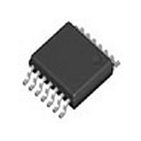
MC74LCX74DTR2G ON Semiconductor, MC74LCX74DTR2G Datasheet - Page 4

MC74LCX74DTR2G
Manufacturer Part Number
MC74LCX74DTR2G
Description
IC FLIP FLOP DUAL D 14-TSSOP
Manufacturer
ON Semiconductor
Series
74LCXr
Type
D-Typer
Datasheet
1.MC74LCX74DR2G.pdf
(8 pages)
Specifications of MC74LCX74DTR2G
Function
Set(Preset) and Reset
Output Type
Differential
Number Of Elements
2
Number Of Bits Per Element
1
Frequency - Clock
150MHz
Delay Time - Propagation
1.5ns
Trigger Type
Positive Edge
Current - Output High, Low
24mA, 24mA
Voltage - Supply
2 V ~ 3.6 V
Operating Temperature
-40°C ~ 85°C
Mounting Type
Surface Mount
Package / Case
14-TSSOP
Logic Family
LCX
Technology
CMOS
Number Of Bits
2
Number Of Elements
2
Clock-edge Trigger Type
Positive-Edge
Polarity
Invert/Non-Invert
Operating Supply Voltage (typ)
2.5/3.3V
Package Type
TSSOP
Propagation Delay Time
8.4ns
Low Level Output Current
24mA
High Level Output Current
-24mA
Operating Supply Voltage (min)
2V
Operating Supply Voltage (max)
3.6V
Operating Temp Range
-40C to 85C
Operating Temperature Classification
Industrial
Mounting
Surface Mount
Pin Count
14
Lead Free Status / RoHS Status
Lead free / RoHS Compliant
Available stocks
Company
Part Number
Manufacturer
Quantity
Price
Company:
Part Number:
MC74LCX74DTR2G
Manufacturer:
ON Semiconductor
Quantity:
1 450
Company:
Part Number:
MC74LCX74DTR2G(LCX74)
Manufacturer:
ITS
Quantity:
6
2. These values of V
3. Skew is defined as the absolute value of the difference between the actual propagation delay for any two separate outputs of the same device.
DC ELECTRICAL CHARACTERISTICS
AC CHARACTERISTICS
Symbol
Symbol
V
V
V
V
I
I
DI
f
t
t
t
t
t
t
t
t
t
t
I
CC
max
PLH
PHL
PLH
PHL
s
h
w
rec
OSHL
OSLH
The specification applies to any outputs switching in the same direction, either HIGH−to−LOW (t
guaranteed by design.
IH
IL
OH
OL
CC
Clock Pulse Frequency
Propagation Delay
CPn to On or On
Propagation Delay
SDn or CDn to On or On
Setup Time, HIGH or LOW Dn to CPn
Hold Time, HIGH or LOW Dn to CPn
CPn Pulse Width, HIGH or LOW
SDn or CDn Pulse Width, LOW
Recovery Time SDn or CDn to CPn
Output−to−Output Skew
(Note 3)
HIGH Level Input Voltage (Note 2)
LOW Level Input Voltage (Note 2)
HIGH Level Output Voltage
LOW Level Output Voltage
Input Leakage Current
Quiescent Supply Current
Increase in I
I
are used to test DC electrical characteristics only.
Characteristic
Parameter
CC
per Input
t
R
= t
F
= 2.5 ns; R
L
= 500 W
Waveform
2.3 V
2.7 V
2.3 V
2.7 V
2.3 V
V
V
V
V
2.3 V
V
V
V
V
2.3 V
2.3
2.3
2.3
1
1
2
1
1
4
3
CC
CC
CC
CC
CC
CC
CC
CC
http://onsemi.com
MC74LCX74
= 2.3 V; I
= 2.7 V; I
= 3.0 V; I
= 3.0 V; I
= 2.3 V; I
= 2.7 V; I
= 3.0 V; I
= 3.0 V; I
V
V
V
CC
CC
CC
V
V
V
V
V
V
V
CC
CC
CC
CC
CC
CC
CC
V
CC
3.6 V; V
3.6 V; 3.6
3.6 V; V
Min
150
1.5
1.5
1.5
1.5
2.5
1.5
3.3
3.3
2.5
4
OH
OH
OH
OH
OL
OL
OL
OL
2.7 V
3.6 V
2.7 V
3.6 V
3.6 V; I
3.6 V; I
3.6 V; 0 V
C
= 3.3 V + 0.3 V
L
Condition
= 8 mA
= 12 mA
= 16 mA
= 24 mA
= −8 mA
= −12 mA
= −18 mA
= −24 mA
= 50 pF
I
IH
= GND or V
OH
OL
= V
Max
7.0
7.0
7.0
7.0
1.0
1.0
V
= 100 mA
= −100 mA
I
CC
V
or V
I
− 0.6 V
O
5.5 V
T
A
CC
Min
150
= −40 C to +85 C
5.5 V
1.5
1.5
1.5
1.5
2.5
1.5
3.3
3.6
3.0
V
C
CC
L
Limits
= 50 pF
OSHL
= 2.7 V
) or LOW−to−HIGH (t
Max
8.0
8.0
8.0
8.0
V
T
CC
A
Min
1.7
2.0
1.8
2.2
2.4
2.2
= −40 C to +85 C
− 0.2
V
CC
Min
150
1.5
1.5
1.5
1.5
4.0
2.0
4.0
4.0
4.5
C
= 2.5 V + 0.2 V
L
= 30 pF
Max
0.55
500
0.7
0.8
0.2
0.6
0.4
0.4
10
10
5
OSLH
Max
8.4
8.4
8.4
8.4
); parameter
Unit
mA
mA
mA
V
V
V
V
MHz
Unit
ns
ns
ns
ns
ns
ns
ns
ns


