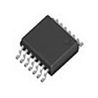
MC74LCX74DTR2G ON Semiconductor, MC74LCX74DTR2G Datasheet - Page 2

MC74LCX74DTR2G
Manufacturer Part Number
MC74LCX74DTR2G
Description
IC FLIP FLOP DUAL D 14-TSSOP
Manufacturer
ON Semiconductor
Series
74LCXr
Type
D-Typer
Datasheet
1.MC74LCX74DR2G.pdf
(8 pages)
Specifications of MC74LCX74DTR2G
Function
Set(Preset) and Reset
Output Type
Differential
Number Of Elements
2
Number Of Bits Per Element
1
Frequency - Clock
150MHz
Delay Time - Propagation
1.5ns
Trigger Type
Positive Edge
Current - Output High, Low
24mA, 24mA
Voltage - Supply
2 V ~ 3.6 V
Operating Temperature
-40°C ~ 85°C
Mounting Type
Surface Mount
Package / Case
14-TSSOP
Logic Family
LCX
Technology
CMOS
Number Of Bits
2
Number Of Elements
2
Clock-edge Trigger Type
Positive-Edge
Polarity
Invert/Non-Invert
Operating Supply Voltage (typ)
2.5/3.3V
Package Type
TSSOP
Propagation Delay Time
8.4ns
Low Level Output Current
24mA
High Level Output Current
-24mA
Operating Supply Voltage (min)
2V
Operating Supply Voltage (max)
3.6V
Operating Temp Range
-40C to 85C
Operating Temperature Classification
Industrial
Mounting
Surface Mount
Pin Count
14
Lead Free Status / RoHS Status
Lead free / RoHS Compliant
Available stocks
Company
Part Number
Manufacturer
Quantity
Price
Company:
Part Number:
MC74LCX74DTR2G
Manufacturer:
ON Semiconductor
Quantity:
1 450
Company:
Part Number:
MC74LCX74DTR2G(LCX74)
Manufacturer:
ITS
Quantity:
6
H
h
L
l
NC = No Change
X
For I
PIN NAMES
TRUTH TABLE
CP1, CP2
D1−D2
CD1, CD2
SD1, SD2
On−On
SDn
H
H
H
H
L
L
CC
= High Voltage Level
= High Voltage Level One Setup Time Prior to the Low−to−High Clock Transition
= Low Voltage Level
= Low Voltage Level One Setup Time Prior to the Low−to−High Clock Transition
= High or Low Voltage Level and Transitions are Acceptable
= Low−to−High Transition
= Not a Low−to−High Transition
reasons, DO NOT FLOAT Inputs
CD1
V
Figure 1. Pinout: 14−Lead (Top View)
14
CC
1
Pins
CDn
H
H
H
H
L
L
CD2
D1 CP1
13
Inputs
2
D2
CPn
12
3
X
X
X
CP2 SD2 O2
SD1 O1
Clock Pulse Inputs
Data Inputs
Direct Clear Inputs
Direct Set Inputs
Outputs
11
4
Dn
X
X
X
X
h
l
10
5
Function
O1
9
6
On
NC
H
H
H
L
L
Outputs
GND
O2
8
7
NC
On
H
H
H
L
L
http://onsemi.com
MC74LCX74
SD1
D1
CP1
CD1
SD2
D2
CP2
CD2
L
Load and Read Register
2
Asynchronous Clear
4
2
3
1
10
12
11
13
Asynchronous Set
Operating Mode
d
Undetermined
d R
Hold
d R
Figure 2. Logic Diagram
i t
CP
CP
D
D
SD
SD
CD
CD
Q
Q
Q
Q
5
6
9
8
O1
O1
O2
O2


