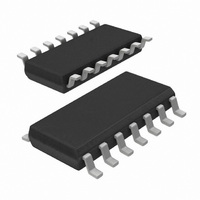
74LVT74D,112 NXP Semiconductors, 74LVT74D,112 Datasheet - Page 2

74LVT74D,112
Manufacturer Part Number
74LVT74D,112
Description
IC 3.3V DUAL D F-F 14SOIC
Manufacturer
NXP Semiconductors
Series
74LVTr
Type
D-Typer
Datasheet
1.74LVT74D118.pdf
(10 pages)
Specifications of 74LVT74D,112
Function
Set(Preset) and Reset
Output Type
Differential
Number Of Elements
2
Number Of Bits Per Element
1
Frequency - Clock
345MHz
Delay Time - Propagation
3.1ns
Trigger Type
Positive Edge
Current - Output High, Low
20mA, 32mA
Voltage - Supply
2.7 V ~ 3.6 V
Operating Temperature
-40°C ~ 85°C
Mounting Type
Surface Mount
Package / Case
14-SOIC (3.9mm Width), 14-SOL
Lead Free Status / RoHS Status
Lead free / RoHS Compliant
Other names
74LVT74D
74LVT74D
935209250112
74LVT74D
935209250112
Philips Semiconductors
QUICK REFERENCE DATA
PIN CONFIGURATION
LOGIC SYMBOL
ORDERING INFORMATION
SYMBOL
14-Pin Plastic SO
14-Pin Plastic SSOP
14-Pin Plastic TSSOP
1996 Aug 28
V
GND = Pin 7
3.3V Dual D-type flip-flop
CC
t
t
C
I
PLH
PHL
CC
= Pin 14
IN
PACKAGES
Propagation
delay
CPn to Qn
Input
capacitance
Total supply
current
PARAMETER
10
13
11
3
4
1
GND
RD0
CP0
SD0
Q0
Q0
D0
1
2
3
4
5
6
7
CP0
SD0
RD0
CP1
SD1
RD1
Q0 Q0 Q1 Q1
C
V
V
5
V
L
CC
I
CONDITIONS
CC
T
= 0V or 3.0V
D0 D1
= 50pF;
6
amb
2
GND = 0V
= 3.3V
= 3.6V
12
9
= 25 C;
TEMPERATURE RANGE
8
14
13
12
11
10
9
8
–40 C to +85 C
–40 C to +85 C
–40 C to +85 C
V
RD1
D1
CP1
SD1
Q1
Q1
CC
TYPICAL
3.1
3.6
0.5
3
SF00045
SA00359
UNIT
mA
ns
pF
OUTSIDE NORTH AMERICA
2
DESCRIPTION
The 74LVT74 is a dual positive edge-triggered D-type flip-flop
featuring individual data, clock, set, and reset inputs; also true and
complementary outputs. Set (SD) and reset (RD) are asynchronous
active low inputs and operate independently of the clock input.
When set and reset are inactive (high), data at the D input is
transferred to the Q and Q outputs on the low-to-high transition of
the clock. Data must be stable just one setup time prior to the
low-to-high transition of the clock for predictable operation. Clock
triggering occurs at a voltage level and is not directly related to the
transition time of the positive-going pulse. Following the hold time
interval, data at the D input may be changed without affecting the
levels of the output.
PIN DESCRIPTION
LOGIC SYMBOL (IEEE/IEC)
74LVT74 PW
74LVT74 DB
PIN NUMBER
74LVT74 D
5, 6, 8, 9
2, 12
3, 11
4, 10
1, 13
12
13
10
11
4
3
2
1
RD0, RD1
CP0, CP1
SD0, SD1
SYMBOL
Qn, Qn
D0, D1
NORTH AMERICA
1D
74LVT74PW DH
S
S
R
2D
R
74LVT74 DB
C1
C2
74LVT74 D
Data inputs
Clock inputs (active rising edge)
Set inputs (active LOW)
Reset inputs (active LOW)
Data outputs
&
NAME AND FUNCTION
Product specification
74LVT74
DWG NUMBER
853-1872 17244
5
6
9
8
SOT108-1
SOT337-1
SOT402-1
SF00047


