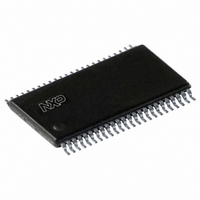
74LVT162374DGG,512 NXP Semiconductors, 74LVT162374DGG,512 Datasheet

74LVT162374DGG,512
Specifications of 74LVT162374DGG,512
74LVT162374DG
935264167512
Related parts for 74LVT162374DGG,512
74LVT162374DGG,512 Summary of contents
Page 1
V 16-bit edge-triggered D-type flip-flop with 30 termination resistors; 3-state Rev. 03 — 17 January 2005 1. General description The 74LVT162374 is a high performance BiCMOS product designed for V 3.3 V. The 74LVT162374 is designed with 30 ...
Page 2
Philips Semiconductors 3. Quick reference data Table amb Symbol PLH PHL Ordering information Table 2: Ordering information Type number Package Temperature range Name 74LVT162374DGG 40 ...
Page 3
Philips Semiconductors 5. Functional diagram 1D0 1D1 1D2 1D3 48 1CP 1 1OE 1Q0 1Q1 1Q2 1Q3 1Q4 1Q5 1Q6 1Q7 2D0 2D1 2D2 2D3 25 2CP 24 ...
Page 4
Philips Semiconductors Fig 4. Output schematic (one output) 6. Pinning information 6.1 Pinning Fig 5. Pin configuration 9397 750 14401 Product data sheet 3.3 V 16-bit edge-triggered D-type flip-fl output 27 001aac372 1 1OE 2 1Q0 1Q1 ...
Page 5
Philips Semiconductors 6.2 Pin description Table 3: Symbol 1OE 1Q0 1Q1 GND 1Q2 1Q3 V CC 1Q4 1Q5 GND 1Q6 1Q7 2Q0 2Q1 GND 2Q2 2Q3 V CC 2Q4 2Q5 GND 2Q6 2Q7 2OE 2CP 2D7 2D6 GND 2D5 2D4 ...
Page 6
Philips Semiconductors Table 3: Symbol 1D5 1D4 V CC 1D3 1D2 GND 1D1 1D0 1CP 7. Functional description 7.1 Function table Table 4: Operating mode Load and read register Hold Disable outputs [ HIGH voltage level ...
Page 7
Philips Semiconductors Table 5: In accordance with the Absolute Maximum Rating System (IEC 60134). Voltages are referenced to GND (ground = 0 V) Symbol stg T j [1] The input and output negative voltage ratings may be ...
Page 8
Philips Semiconductors Table 7: Static characteristics At recommended operating conditions; voltages are referenced to GND (ground = 0 V). Symbol Parameter I bus hold current D inputs HOLD I external current into output power-up or power-down ...
Page 9
Philips Semiconductors Table 8: Dynamic characteristics GND = 2 Symbol Parameter t propagation delay PHL nCP to nQn t output enable time to PZH HIGH-level ...
Page 10
Philips Semiconductors 12. Waveforms Fig 6. Propagation delay clock input to output, clock pulse width and maximum clock Fig 7. 3-state output enable time to HIGH-level and output disable time from HIGH-level Fig 8. 3-state output enable time to LOW-level ...
Page 11
Philips Semiconductors Fig 9. Data set-up and hold times a. Input pulse definition b. Test circuit Fig 10. Load circuitry for switching times 9397 750 14401 Product data sheet nDn su(H) h(H) nCP V ...
Page 12
Philips Semiconductors Table 10: Supply voltage 2.7 V 9397 750 14401 Product data sheet Test data Repetition rate Input MHz 500 ns 2 Rev. 03 — 17 January 2005 ...
Page 13
Philips Semiconductors 13. Package outline TSSOP48: plastic thin shrink small outline package; 48 leads; body width 6 pin 1 index 1 DIMENSIONS (mm are the original dimensions). A UNIT max. ...
Page 14
Philips Semiconductors SSOP48: plastic shrink small outline package; 48 leads; body width 7 pin 1 index 1 e DIMENSIONS (mm are the original dimensions) A UNIT max. 0.4 2.35 mm ...
Page 15
Philips Semiconductors 14. Revision history Table 11: Revision history Document ID Release date 74LVT162374_3 20050117 • Modifications: The format of this data sheet is redesigned to comply with the current presentation and information standard of Philips Semiconductors. • Section 2 ...
Page 16
Philips Semiconductors 15. Data sheet status [1] Level Data sheet status Product status I Objective data Development II Preliminary data Qualification III Product data Production [1] Please consult the most recently issued data sheet before initiating or completing a design. ...
Page 17
Philips Semiconductors 19. Contents 1 General description . . . . . . . . . . . . . . . . . . . . . . 1 2 Features . . . . . . . . ...


