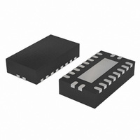
74LVT273BQ,115 NXP Semiconductors, 74LVT273BQ,115 Datasheet - Page 5

74LVT273BQ,115
Manufacturer Part Number
74LVT273BQ,115
Description
IC 3.3V OCTAL D FF 20-DHVQFN
Manufacturer
NXP Semiconductors
Series
74LVTr
Type
D-Type Busr
Datasheet
1.74LVT273D112.pdf
(17 pages)
Specifications of 74LVT273BQ,115
Function
Master Reset
Output Type
Non-Inverted
Number Of Elements
1
Number Of Bits Per Element
8
Frequency - Clock
150MHz
Delay Time - Propagation
3.5ns
Trigger Type
Positive Edge
Current - Output High, Low
32mA, 64mA
Voltage - Supply
2.7 V ~ 3.6 V
Operating Temperature
-40°C ~ 85°C
Mounting Type
Surface Mount
Package / Case
20-VQFN Exposed Pad, 20-HVQFN, 20-SQFN, 20-DHVQFN
Number Of Circuits
8
Logic Family
74LVT
Logic Type
BiCMOS
Polarity
Non-Inverting
Input Type
Single-Ended
Propagation Delay Time
3.5 ns
High Level Output Current
- 32 mA
Supply Voltage (max)
3.6 V
Maximum Operating Temperature
+ 85 C
Mounting Style
SMD/SMT
Minimum Operating Temperature
- 40 C
Supply Voltage (min)
2.7 V
Lead Free Status / RoHS Status
Lead free / RoHS Compliant
Lead Free Status / RoHS Status
Lead free / RoHS Compliant, Lead free / RoHS Compliant
Other names
74LVT273BQ-G
74LVT273BQ-G
935285606115
74LVT273BQ-G
935285606115
NXP Semiconductors
6. Functional description
Table 3.
[1]
7. Limiting values
Table 4.
In accordance with the Absolute Maximum Rating System (IEC 60134). Voltages are referenced to GND (ground = 0 V).
[1]
[2]
[3]
8. Recommended operating conditions
Table 5.
74LVT273_3
Product data sheet
Inputs
MR
L
H
H
H
Symbol
V
V
V
I
I
I
T
T
P
Symbol
V
V
I
IK
OK
O
OH
stg
j
CC
I
O
tot
CC
I
H = HIGH voltage level; h = HIGH voltage level one set-up time prior to the prior to the LOW-to-HIGH clock transition;
L = LOW voltage level; l = LOW voltage level one set-up time prior to the prior to the LOW-to-HIGH clock transition;
X = Don’t care;
The input and output negative voltage ratings may be exceeded if the input and output clamp current ratings are observed.
The performance capability of a high-performance integrated circuit in conjunction with its thermal environment can create junction
temperatures which are detrimental to reliability.
For SO20 packages: above 70 C derate linearly with 8 mW/K.
For SSOP20 and TSSOP20 packages: above 60 C derate linearly with 5.5 mW/K.
For DHVQFN20 packages: above 60 C derate linearly with 4.5 mW/K.
Parameter
supply voltage
input voltage
HIGH-level output current
Function selection
Limiting values
Recommended operating conditions
Parameter
supply voltage
input voltage
output voltage
input clamping current
output clamping current
output current
storage temperature
junction temperature
total power dissipation
= LOW-to-HIGH clock transition; Q0 = output as it was.
CP
X
L
Conditions
Output in OFF or HIGH state
V
V
output in LOW state
output in HIGH state
T
amb
I
O
Rev. 03 — 10 September 2008
< 0 V
< 0 V
Dn
X
h
l
X
Conditions
= 40 C to +85 C
Outputs
Qn
L
H
L
Q0
Min
2.7
0
32
[1]
[1]
[2]
[3]
Min
-
-
0.5
0.5
0.5
50
64
65
50
Typ
-
-
-
3.3 V octal D-type flip-flop
Max
+4.6
+7.0
+7.0
-
-
128
-
+150
150
500
Operating mode
Reset (clear)
Load 1
Load 0
Retain state
74LVT273
Max
3.6
5.5
-
© NXP B.V. 2008. All rights reserved.
Unit
V
V
V
mA
mA
mA
mA
mW
Unit
V
V
mA
C
C
5 of 17


