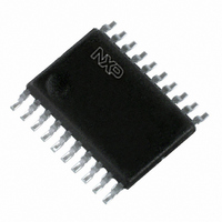
74ABT574APW,112 NXP Semiconductors, 74ABT574APW,112 Datasheet - Page 5

74ABT574APW,112
Manufacturer Part Number
74ABT574APW,112
Description
IC OCTAL D-TYPE F-F 3-ST 20TSSOP
Manufacturer
NXP Semiconductors
Series
74ABTr
Type
D-Type Busr
Datasheet
1.74ABT574ADB118.pdf
(11 pages)
Specifications of 74ABT574APW,112
Function
Standard
Output Type
Tri-State Non Inverted
Number Of Elements
1
Number Of Bits Per Element
8
Frequency - Clock
400MHz
Delay Time - Propagation
3ns
Trigger Type
Positive Edge
Current - Output High, Low
32mA, 64mA
Voltage - Supply
4.5 V ~ 5.5 V
Operating Temperature
-40°C ~ 85°C
Mounting Type
Surface Mount
Package / Case
20-TSSOP
Lead Free Status / RoHS Status
Lead free / RoHS Compliant
Other names
74ABT574APW
74ABT574APW
935199960112
74ABT574APW
935199960112
1. Not more than one output should be tested at a time, and the duration of the test should not exceed one second.
2. This is the increase in supply current for each input at 3.4V.
3. For valid test results, data must not be loaded into the flip-flops (or latches) after applying the power.
4. This parameter is valid for any V
Philips Semiconductors
DC ELECTRICAL CHARACTERISTICS
NOTES:
AC CHARACTERISTICS
GND = 0V, t
1995 May 22
SYMBOL
SYMBOL
f
t
t
t
t
t
t
MAX
PLH
PHL
PZH
PZL
PHZ
PLZ
Octal D-type flip-flop (3-State)
I
transition time of up to 100 sec is permitted.
PU
V
I
I
V
I
I
I
I
I
V
V
OFF
OZH
CEX
CCH
CCL
CCZ
OZL
RST
I
I
OH
OL
I
/I
O
CC
IK
I
PD
R
Input clamp voltage
High-level output voltage
Low-level output voltage
Power-up output low
voltage
Input leakage current
Power-off leakage current
Power-up/down 3-State
output current
3-State output High current
3-State output Low current
Output High leakage current
Output current
Quiescent supply current
Additional supply current per
input pin
= t
Maximum clock frequency
Propagation delay
CP to Qn
Output enable time
to High and Low level
Output disable time
from High and Low level
F
= 2.5ns, C
3
PARAMETER
PARAMETER
2
4
1
L
= 50pF, R
CC
between 0V and 2.1V, with a transition time of up to 10 msec. From V
L
= 500
V
V
V
V
V
V
V
V
V
V
V
V
V
V
V
V
V
V
V
other inputs at V
CC
CC
CC
CC
CC
CC
CC
CC
CC
OE
CC
CC
CC
CC
CC
CC
CC
I
CC
= GND or V
WAVEFORM
= 4.5V; I
= 4.5V; I
= 5.0V; I
= 4.5V; I
= 4.5V; I
= 5.5V; I
= 5.5V; V
= 0.0V; V
= 2.0V; V
= Don’t care
= 5.5V; V
= 5.5V; V
= 5.5V; V
= 5.5V; V
= 5.5V; Outputs High, V
= 5.5V; Outputs Low, V
= 5.5V; Outputs 3-State;
= 5.5V; one input at 3.4V,
1
1
3
4
3
4
TEST CONDITIONS
IK
OH
OH
OH
OL
O
I
O
O
O
O
O
O
CC
= 1mA; V
= GND or 5.5V
= –18mA
or V
= 0.5V; V
= 2.7V; V
= 0.5V; V
= 5.5V; V
= 2.5V
= 64mA; V
= –32mA; V
CC
= –3mA; V
= –3mA; V
or GND
I
4.5V
I
I
I
I
I
= GND or V
5
= GND or V
= V
= V
= GND or V
I
I
I
Min
150
1.5
2.0
1.0
2.5
1.8
1.4
= V
I
= V
= V
I
I
= GND or V
= V
= GND or V
IL
IL
IL
IL
IL
or V
or V
IL
or V
T
or V
or V
V
amb
or V
CC
IH
IH
CC
IH
IH
IH
CC;
CC
Typ
400
3.0
3.4
2.9
3.8
3.1
2.6
IH
= +5.0V
= +25
CC
CC
o
C
Min
–40
2.5
3.0
2.0
LIMITS
Min
4.4
4.7
4.1
5.2
4.3
3.8
T
amb
–0.9
0.42
0.13
–5.0
Typ
100
100
2.9
3.4
2.4
0.01
5.0
5.0
0.5
= +25 C
24
5.0
5.0
T
V
amb
Min
150
CC
CC
1.5
2.0
1.0
2.5
1.8
1.4
LIMITS
–180
Max
–1.2
0.55
0.55
–50
250
250
= 2.1V to V
= -40 to +85
= +5.0V 0.5V
1.5
100
50
50
30
1.0
50
T
74ABT574A
Min
–40
amb
2.5
3.0
2.0
Max
5.0
5.1
5.0
5.7
5.0
4.0
to +85 C
CC
Product specification
o
= –40 C
C
= 5V "10% a
–180
Max
–1.2
0.55
0.55
–50
250
250
1.5
100
50
50
30
1.0
50
UNIT
ns
ns
ns
ns
UNIT
mA
mA
mA
V
V
V
V
V
V
A
A
A
A
A
A
A
A


