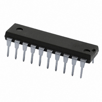
N74F273AN,602 NXP Semiconductors, N74F273AN,602 Datasheet - Page 3

N74F273AN,602
Manufacturer Part Number
N74F273AN,602
Description
IC FLIP FLOP OCTAL D 25MA 20DIP
Manufacturer
NXP Semiconductors
Series
74Fr
Type
D-Type Busr
Datasheet
1.N74F273AD623.pdf
(10 pages)
Specifications of N74F273AN,602
Function
Master Reset
Output Type
Non-Inverted
Number Of Elements
1
Number Of Bits Per Element
8
Frequency - Clock
170MHz
Delay Time - Propagation
7ns
Trigger Type
Positive Edge
Current - Output High, Low
1mA, 20mA
Voltage - Supply
4.5 V ~ 5.5 V
Operating Temperature
0°C ~ 70°C
Mounting Type
Through Hole
Package / Case
20-DIP (0.300", 7.62mm)
Number Of Circuits
1
Logic Family
F
Logic Type
D-Type Edge Triggered Flip-Flop
Polarity
Non-Inverting
Input Type
Single-Ended
Propagation Delay Time
7 ns
High Level Output Current
- 1 mA
Supply Voltage (max)
5.5 V
Maximum Operating Temperature
+ 70 C
Mounting Style
Through Hole
Minimum Operating Temperature
0 C
Supply Voltage (min)
4.5 V
Technology
Bipolar
Number Of Bits
8
Number Of Elements
1
Clock-edge Trigger Type
Positive-Edge
Operating Supply Voltage (typ)
5V
Package Type
PDIP
Low Level Output Current
20mA
Frequency (max)
125MHz
Operating Supply Voltage (min)
4.5V
Operating Supply Voltage (max)
5.5V
Operating Temp Range
0C to 70C
Operating Temperature Classification
Commercial
Mounting
Through Hole
Pin Count
20
Lead Free Status / RoHS Status
Lead free / RoHS Compliant
Lead Free Status / RoHS Status
Lead free / RoHS Compliant, Lead free / RoHS Compliant
Other names
568-1725-5
935053570602
N74F273AN
935053570602
N74F273AN
Available stocks
Company
Part Number
Manufacturer
Quantity
Price
Company:
Part Number:
N74F273AN,602
Manufacturer:
VISHAY
Quantity:
9 755
H = High voltage level
h = High voltage level one set–up time prior to the Low–to–High clock transition
L = Low voltage level
l
X = Don’t care
Philips Semiconductors
LOGIC SYMBOL (IEEE/IEC)
LOGIC DIAGRAM
FUNCTION TABLE
1996 Mar 12
Octal D flip–flop
V
GND = Pin 10
= Low voltage level one set–up time prior to the Low–to–High clock transition
= Low–to–High clock transition
MR
CP
CC
= Pin 20
1
11
MR
H
H
L
1
11
3
4
7
8
13
14
17
18
D0
3
D
CP
R
D
1D
R
Q
C1
Q0
2
INPUTS
D1
CP
X
4
D
CP
R
D
Q
SF00348
Q1
5
2
5
6
9
12
15
16
19
D2
7
D
CP
R
D
Q
Dn
X
h
l
Q2
6
D3
8
D
CP
R
3
D
Q
Q3
9
OUTPUTS
D4
Q0 – Q7
13
H
D
L
L
CP
R
D
Q
Q4
12
D5
14
Reset (clear)
Load ”1”
Load ”0”
D
CP
R
D
Q
Q5
15
D6
17
OPERATING
D
CP
R
MODE
D
Q
Q6
Product specification
16
74F273A
D7
18
D
CP
R
D
Q
SF00349
Q7
19


