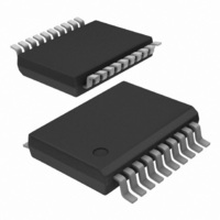
74LVT574DB,112 NXP Semiconductors, 74LVT574DB,112 Datasheet - Page 4

74LVT574DB,112
Manufacturer Part Number
74LVT574DB,112
Description
IC OCTAL D TRANSP F-F 20SSOP
Manufacturer
NXP Semiconductors
Series
74LVTr
Type
D-Type Busr
Datasheet
1.74LVT574PW118.pdf
(16 pages)
Specifications of 74LVT574DB,112
Function
Standard
Output Type
Tri-State Non Inverted
Number Of Elements
1
Number Of Bits Per Element
8
Frequency - Clock
150MHz
Delay Time - Propagation
3.6ns
Trigger Type
Positive Edge
Current - Output High, Low
32mA, 64mA
Voltage - Supply
2.7 V ~ 3.6 V
Operating Temperature
-40°C ~ 85°C
Mounting Type
Surface Mount
Package / Case
20-SSOP
Logic Family
LVT
Technology
BiCMOS
Number Of Bits
8
Number Of Elements
1
Clock-edge Trigger Type
Positive-Edge
Polarity
Non-Inverting
Operating Supply Voltage (typ)
3.3V
Package Type
SSOP
Propagation Delay Time
6.6ns
Low Level Output Current
64mA
High Level Output Current
-32mA
Frequency (max)
150MHz
Operating Supply Voltage (min)
2.7V
Operating Supply Voltage (max)
3.6V
Operating Temp Range
-40C to 85C
Operating Temperature Classification
Industrial
Mounting
Surface Mount
Pin Count
20
Lead Free Status / RoHS Status
Lead free / RoHS Compliant
Other names
74LVT574DB
74LVT574DB
935170730112
74LVT574DB
935170730112
NXP Semiconductors
6. Functional description
Table 3.
[1]
7. Limiting values
Table 4.
In accordance with the Absolute Maximum Rating System (IEC 60134). Voltages are referenced to GND (ground = 0 V).
[1]
[2]
[3]
74LVT_LVTH574_4
Product data sheet
Operating mode
Load and read register
Hold
Disable outputs
Symbol
V
V
V
I
I
I
T
T
P
IK
OK
O
stg
j
CC
I
O
tot
H = HIGH voltage level;
L = LOW voltage level;
h = HIGH voltage level one setup time prior to the LOW-to-HIGH clock transition;
l = LOW voltage level one setup time prior to the LOW-to-HIGH clock transition;
Z = high-impedance OFF-state;
NC = no change;
X = don’t care.
The input and output negative voltage ratings may be exceeded if the input and output clamp current ratings are observed.
The performance capability of a high-performance integrated circuit in conjunction with its thermal environment can create junction
temperatures which are detrimental to reliability.
For SO20 packages: above 70 ˚C derate linearly with 8 mW/K.
For SSOP20 and TSSOP20 packages: above 60 ˚C derate linearly with 5.5 mW/K.
For DHVQFN20 packages: above 60 ˚C derate linearly with 4.5 mW/K.
= LOW-to-HIGH clock transition;
Function table
Limiting values
Parameter
supply voltage
input voltage
output voltage
input clamping current
output clamping current
output current
storage temperature
junction temperature
total power dissipation
6.1 Function table
[1]
Control
OE
L
L
H
Conditions
output in OFF-state or HIGH-state
V
V
output in LOW-state
output in HIGH-state
T
amb
I
O
Rev. 04 — 11 September 2008
< 0 V
CP
NC
X
< 0 V
= -40 ˚C to +85 ˚C
Input
Dn
l
h
X
X
74LVT574; 74LVTH574
3.3 V octal D-type flip-flop; 3-state
Internal register Output
L
H
NC
NC
[1]
[1]
[2]
Min
-
-
-
-
-
-
0.5
0.5
0.5
65
Max
+4.6
+7.0
+7.0
128
+150
150
500
© NXP B.V. 2008. All rights reserved.
50
50
64
Qn
L
H
NC
Z
Unit
V
V
V
mA
mA
mA
mA
mW
C
C
4 of 16


