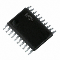
74LVT273PW,112 NXP Semiconductors, 74LVT273PW,112 Datasheet - Page 7

74LVT273PW,112
Manufacturer Part Number
74LVT273PW,112
Description
IC 3.3V OCTAL D FF 20TSSOP
Manufacturer
NXP Semiconductors
Series
74LVTr
Type
D-Type Busr
Datasheet
1.74LVT273D112.pdf
(17 pages)
Specifications of 74LVT273PW,112
Function
Master Reset
Output Type
Non-Inverted
Number Of Elements
1
Number Of Bits Per Element
8
Frequency - Clock
150MHz
Delay Time - Propagation
3.5ns
Trigger Type
Positive Edge
Current - Output High, Low
32mA, 64mA
Voltage - Supply
2.7 V ~ 3.6 V
Operating Temperature
-40°C ~ 85°C
Mounting Type
Surface Mount
Package / Case
20-TSSOP
Lead Free Status / RoHS Status
Lead free / RoHS Compliant
Other names
74LVT273PW
74LVT273PW
935176350112
74LVT273PW
935176350112
NXP Semiconductors
Table 6.
At recommended operating conditions. Voltages are referenced to GND (ground = 0 V).
[1]
[2]
[3]
[4]
[5]
10. Dynamic characteristics
Table 7.
Voltages are referenced to GND (ground = 0 V). For test circuit see
74LVT273_3
Product data sheet
Symbol Parameter
I
C
Symbol Parameter
t
t
t
t
CC
PLH
PHL
su
h
I
I
CC
All typical values are measured at V
For valid test results data must not be loaded into the flip-flops (or latches) after applying the power.
Unused pins at V
This is the bus hold overdrive current required to force the input to the opposite logic state.
Increase in supply current for each input at the specified voltage level other than V
supply current
additional supply current
input capacitance
LOW to HIGH propagation delay
HIGH to LOW propagation delay
set-up time
hold time
Static characteristics
Dynamic characteristics
CC
or GND.
…continued
CC
= 3.3 V (unless stated otherwise) and T
Conditions
V
per input pin; V
one input = V
other inputs at V
V
CC
I
outputs HIGH
outputs LOW
= 0 V or 3.0 V
= 3.6 V; V
Conditions
CP to Qn;
CP to Qn;
MR to Qn; see
Dn to CP HIGH; see
Dn to CP LOW; see
Dn to CP HIGH; see
Dn to CP LOW; see
Rev. 03 — 10 September 2008
V
V
V
V
V
V
V
V
V
V
V
V
V
V
CC
CC
CC
CC
CC
CC
CC
CC
CC
CC
CC
CC
CC
CC
= 2.7 V
= 3.3 V
= 2.7 V
= 3.3 V
= 2.7 V
= 3.3 V
= 2.7 V
= 3.3 V
= 2.7 V
= 3.3 V
= 2.7 V
= 3.3 V
= 2.7 V
= 3.3 V
CC
I
CC
= V
CC
Figure 6
Figure 6
= 3.0 V to 3.6 V;
0.6 V
CC
or GND
Figure 7
or GND; I
0.3 V
0.3 V
0.3 V
0.3 V
0.3 V
0.3 V
0.3 V
Figure
Figure 7
Figure 8
Figure 7
Figure 8
O
amb
= 0 A
9.
CC
= 25 C.
or GND
[5]
[2]
[3]
Min
-
-
-
-
Min
1.7
1.9
1.3
2.7
2.3
2.7
2.3
3.3 V octal D-type flip-flop
0
0
0
0
-
-
-
40 C to +85 C
40 C to +85 C
Typ
Typ
0.13
74LVT273
3.5
3.5
3.2
1.0
1.0
0.1
0.6
0.6
3
4
-
-
-
-
-
-
-
© NXP B.V. 2008. All rights reserved.
[1]
[1]
Max
6.3
5.5
5.9
5.5
6.2
6.2
Max
0.19
0.2
-
-
-
-
-
-
-
-
12
-
Unit
ns
ns
ns
ns
ns
ns
ns
ns
ns
ns
ns
ns
ns
ns
7 of 17
Unit
mA
mA
mA
pF


