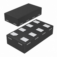
74AUP1G74GD,125 NXP Semiconductors, 74AUP1G74GD,125 Datasheet - Page 16

74AUP1G74GD,125
Manufacturer Part Number
74AUP1G74GD,125
Description
IC FLIP-FLOP D POS-EDGE 8-XSON
Manufacturer
NXP Semiconductors
Series
74AUPr
Type
D-Typer
Datasheet
1.74AUP1G74GM125.pdf
(28 pages)
Specifications of 74AUP1G74GD,125
Output Type
Differential
Package / Case
8-XSON
Function
Set(Preset) and Reset
Number Of Elements
1
Number Of Bits Per Element
1
Frequency - Clock
550MHz
Delay Time - Propagation
2.2ns
Trigger Type
Positive Edge
Current - Output High, Low
4mA, 4mA
Voltage - Supply
0.8 V ~ 3.6 V
Operating Temperature
-40°C ~ 125°C
Mounting Type
Surface Mount
Number Of Circuits
1
Logic Family
AUP
Logic Type
CMOS
Polarity
Inverting/Non-Inverting
Input Type
Single-Ended
Propagation Delay Time
22.5 ns
High Level Output Current
- 4 mA
Low Level Output Current
4 mA
Supply Voltage (max)
3.6 V
Maximum Operating Temperature
+ 125 C
Mounting Style
SMD/SMT
Minimum Operating Temperature
- 40 C
Supply Voltage (min)
0.8 V
Lead Free Status / RoHS Status
Lead free / RoHS Compliant
Lead Free Status / RoHS Status
Lead free / RoHS Compliant, Lead free / RoHS Compliant
Other names
74AUP1G74GD-G
74AUP1G74GD-G
935286839125
74AUP1G74GD-G
935286839125
NXP Semiconductors
74AUP1G74
Product data sheet
Fig 9.
Measurement points are given in
V
The set input (SD) and reset input (RD) to output (Q, Q) propagation delays, the set input (SD) and reset
input (RD) pulse widths and the reset input (RD) to clock input (CP) recovery time
OL
and V
OH
are typical output voltage levels that occur with the output load.
RD input
CP input
SD input
Q output
Q output
GND
GND
GND
V
V
V
V
OH
OH
OL
OL
V
V
V
I
I
I
Table
All information provided in this document is subject to legal disclaimers.
Low-power D-type flip-flop with set and reset; positive-edge trigger
10.
V
M
Rev. 5 — 26 July 2010
t
W
V
V
M
M
t
t
PLH
PHL
V
M
t
W
t
t
PHL
PLH
V
M
t
t
rec
rec
001aae366
74AUP1G74
© NXP B.V. 2010. All rights reserved.
16 of 28


