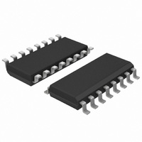
HEF4027BT,653 NXP Semiconductors, HEF4027BT,653 Datasheet - Page 7

HEF4027BT,653
Manufacturer Part Number
HEF4027BT,653
Description
IC DUAL JK FLIP FLOP 16SOIC
Manufacturer
NXP Semiconductors
Series
4000Br
Type
JK Typer
Specifications of HEF4027BT,653
Package / Case
16-SOIC (3.9mm Width)
Function
Set(Preset) and Reset
Output Type
Differential
Number Of Elements
2
Number Of Bits Per Element
1
Frequency - Clock
30MHz
Trigger Type
Positive Edge
Voltage - Supply
3 V ~ 15 V
Operating Temperature
-40°C ~ 85°C
Mounting Type
Surface Mount
Number Of Circuits
2
Logic Family
HEF4000
Logic Type
Dual JK Flip-Flop
Polarity
Inverting/Non-Inverting
Input Type
Single-Ended
Propagation Delay Time
30 ns at 15 V
High Level Output Current
- 3.6 mA
Low Level Output Current
3.6 mA
Supply Voltage (max)
15.5 V
Maximum Operating Temperature
+ 85 C
Mounting Style
SMD/SMT
Minimum Operating Temperature
- 40 C
Supply Voltage (min)
4.5 V
Lead Free Status / RoHS Status
Lead free / RoHS Compliant
Current - Output High, Low
-
Delay Time - Propagation
-
Lead Free Status / Rohs Status
Lead free / RoHS Compliant
Other names
933372790653
HEF4027BTD-T
HEF4027BTD-T
HEF4027BTD-T
HEF4027BTD-T
Available stocks
Company
Part Number
Manufacturer
Quantity
Price
Part Number:
HEF4027BT,653
Manufacturer:
NEXPERIA/安世
Quantity:
20 000
NXP Semiconductors
Table 7.
V
[1]
[2]
Table 8.
P
12. Waveforms
HEF4027B_7
Product data sheet
Symbol Parameter
f
Symbol
P
max
SS
D
Fig 4.
Fig 5.
D
can be calculated from the formulas shown. V
= 0 V; T
The typical values of the propagation delay and transition times are calculated from the extrapolation formulas shown (C
t
t
is the same as t
maximum
frequency
V
Measurement points are given in
Waveforms showing rise, fall and transition times and propagation delays
Measurement points are given in
Waveforms showing set-up and hold times and minimum clock pulse width
OH
Dynamic characteristics
Dynamic power dissipation P
Parameter
dynamic power
dissipation
amb
and V
= 25
OL
TLH
°
C; for test circuit see
are typical output voltages levels that occur with the output load.
and t
THL
.
Conditions
CP input;
J = K = HIGH;
see
CP INPUT
J,K INPUT
V
10 V
15 V
5 V
DD
Figure 5
SD, CD or CP
…continued
OUTPUT
Table
Table
INPUT
Q or Q
V
Typical formula for P
P
P
P
V
Figure
D
0 V
OH
OL
D
D
D
V
9.
9.
I
= 900 × f
= 4500 × f
= 13200 × f
V
t
M
su
Rev. 07 — 25 November 2009
10 %
SS
V
10 V
15 V
7; unless otherwise specified.
5 V
DD
10 %
= 0 V; t
V
M
t
V
h
i
M
V
+ Σ(f
i
90 %
M
+ Σ(f
i
t
+ Σ(f
90 %
r
r
t
= t
PLH
t
o
TLH
1/f
o
× C
Extrapolation formula
f
max
o
× C
≤
× C
D
20 ns; T
L
) × V
(μW)
L
) × V
L
t
) × V
W
t
f
DD
DD
amb
2
DD
2
2
= 25
001aah863
°
C.
t
Where:
f
f
C
V
Σ(f
001aae596
PHL
t
i
o
THL
[1]
DD
= input frequency in MHz;
L
= output frequency in MHz;
o
= output load capacitance in pF;
× C
= supply voltage in V;
Min
L
12
15
) = sum of the outputs.
4
HEF4027B
Typ
25
30
8
© NXP B.V. 2009. All rights reserved.
Dual JK flip-flop
Max
-
-
-
L
in pF).
Unit
MHz
MHz
MHz
7 of 13


