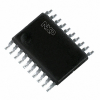
74AHCT574PW,118 NXP Semiconductors, 74AHCT574PW,118 Datasheet - Page 4

74AHCT574PW,118
Manufacturer Part Number
74AHCT574PW,118
Description
IC OCT D FF POS-EDG TRIG 20TSSOP
Manufacturer
NXP Semiconductors
Series
74AHCTr
Type
D-Type Busr
Datasheet
1.74AHC574PW118.pdf
(18 pages)
Specifications of 74AHCT574PW,118
Package / Case
20-TSSOP
Function
Standard
Output Type
Tri-State Non Inverted
Number Of Elements
1
Number Of Bits Per Element
8
Frequency - Clock
115MHz
Delay Time - Propagation
6.3ns
Trigger Type
Positive Edge
Current - Output High, Low
8mA, 8mA
Voltage - Supply
4.5 V ~ 5.5 V
Operating Temperature
-40°C ~ 125°C
Mounting Type
Surface Mount
Number Of Circuits
1
Logic Family
AHCT
Logic Type
D-Type Edge Triggered Flip-Flop
Polarity
Non-Inverting
Input Type
Single-Ended
Propagation Delay Time
4.4 ns
High Level Output Current
- 8 mA
Supply Voltage (max)
5.5 V
Maximum Operating Temperature
+ 125 C
Mounting Style
SMD/SMT
Minimum Operating Temperature
- 40 C
Supply Voltage (min)
4.5 V
Technology
CMOS
Number Of Bits
8
Number Of Elements
1
Clock-edge Trigger Type
Positive-Edge
Operating Supply Voltage (typ)
5V
Package Type
TSSOP
Low Level Output Current
8mA
Frequency (max)
110MHz
Operating Supply Voltage (min)
4.5V
Operating Supply Voltage (max)
5.5V
Operating Temp Range
-40C to 125C
Operating Temperature Classification
Automotive
Mounting
Surface Mount
Pin Count
20
Lead Free Status / RoHS Status
Lead free / RoHS Compliant
Lead Free Status / RoHS Status
Lead free / RoHS Compliant, Lead free / RoHS Compliant
Other names
74AHCT574PW-T
74AHCT574PW-T
935263083118
74AHCT574PW-T
935263083118
Available stocks
Company
Part Number
Manufacturer
Quantity
Price
Company:
Part Number:
74AHCT574PW,118
Manufacturer:
NXP Semiconductors
Quantity:
3 950
NXP Semiconductors
5. Pinning information
Table 2.
74AHC_AHCT574_2
Product data sheet
Symbol
OE
D[0:7]
GND
CP
Q[0:7]
V
Fig 5.
CC
Pin configuration SO20, TSSOP20
Pin description
GND
OE
Pin
1
2, 3, 4, 5, 6, 7, 8, 9
10
11
19, 18, 17, 16, 15, 14, 13, 12 3-state flip-flop output
20
D0
D1
D2
D3
D4
D5
D6
D7
10
1
2
3
4
5
6
7
8
9
5.1 Pinning
5.2 Pin description
74AHCT574
74AHC574
001aah037
20
19
18
17
16
15
14
13
12
11
Description
3-state output enable input (active LOW)
data input
ground (0 V)
clock input (LOW-to-HIGH, edge triggered)
supply voltage
V
Q0
Q1
Q2
Q3
Q4
Q5
Q6
Q7
CP
CC
Rev. 02 — 24 January 2008
Octal D-type flip-flop; positive edge-trigger; 3-state
Fig 6.
74AHC574; 74AHCT574
(1) The die substrate is attached to this pad using
conductive die attach material. It can not be used as a
supply pin or input.
Pin configuration DHVQFN20
index area
terminal 1
D0
D1
D2
D3
D4
D5
D6
D7
Transparent top view
2
3
4
5
6
7
8
9
74AHCT574
74AHC574
GND
(1)
19
18
17
16
15
14
13
12
001aah666
© NXP B.V. 2008. All rights reserved.
Q0
Q1
Q2
Q3
Q4
Q5
Q6
Q7
4 of 18


