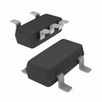
74LVC1G79GV,125 NXP Semiconductors, 74LVC1G79GV,125 Datasheet - Page 4

74LVC1G79GV,125
Manufacturer Part Number
74LVC1G79GV,125
Description
IC SNGL D FF POSEDG TRIG SC74A-5
Manufacturer
NXP Semiconductors
Series
74LVCr
Type
D-Typer
Datasheet
1.74LVC1G79GW125.pdf
(20 pages)
Specifications of 74LVC1G79GV,125
Output Type
Non-Inverted
Package / Case
SC-74-5, SOT-753
Function
Standard
Number Of Elements
1
Number Of Bits Per Element
1
Frequency - Clock
500MHz
Delay Time - Propagation
1.7ns
Trigger Type
Positive Edge
Current - Output High, Low
32mA, 32mA
Voltage - Supply
1.65 V ~ 5.5 V
Operating Temperature
-40°C ~ 125°C
Mounting Type
Surface Mount
Number Of Circuits
1
Logic Family
LVC
Logic Type
D-Type Edge Triggered Flip-Flop
Polarity
Non-Inverting
Input Type
Single-Ended
Propagation Delay Time
2.2 ns at 3.3 V
High Level Output Current
- 32 mA
Low Level Output Current
32 mA
Supply Voltage (max)
5.5 V
Maximum Operating Temperature
+ 125 C
Mounting Style
SMD/SMT
Minimum Operating Temperature
- 40 C
Supply Voltage (min)
1.65 V
Lead Free Status / RoHS Status
Lead free / RoHS Compliant
Lead Free Status / RoHS Status
Lead free / RoHS Compliant, Lead free / RoHS Compliant
Other names
74LVC1G79GV
74LVC1G79GV
935272020125
74LVC1G79GV
935272020125
NXP Semiconductors
7. Functional description
Table 4.
[1]
8. Limiting values
Table 5.
In accordance with the Absolute Maximum Rating System (IEC 60134). Voltages are referenced to GND (ground = 0 V).
[1]
[2]
[3]
74LVC1G79
Product data sheet
Input
CP
↑
↑
L
Symbol
V
I
V
I
V
I
I
I
P
T
IK
OK
O
CC
GND
stg
CC
I
O
tot
H = HIGH voltage level;
L = LOW voltage level;
↑ = LOW-to-HIGH CP transition;
X = don’t care;
q = lower case letter indicates the state of referenced input, one set-up time prior to the LOW-to-HIGH CP transition.
The input and output voltage ratings may be exceeded if the input and output current ratings are observed.
When V
For TSSOP5 and SC-74A packages: above 87.5 °C the value of P
For XSON6 packages: above 118 °C the value of P
CC
Function table
Limiting values
Parameter
supply voltage
input clamping current
input voltage
output clamping current
output voltage
output current
supply current
ground current
total power dissipation
storage temperature
= 0 V (Power-down mode), the output voltage can be 5.5 V in normal operation.
[1]
D
L
H
X
All information provided in this document is subject to legal disclaimers.
V
V
Active mode
V
Conditions
Power-down mode
T
amb
I
O
O
Rev. 8 — 30 September 2010
< 0 V
tot
> V
= 0 V to V
= −40 °C to +125 °C
derates linearly with 7.8 mW/K.
CC
or V
CC
O
< 0 V
tot
derates linearly with 4.0 mW/K.
Single D-type flip-flop; positive-edge trigger
Output
Q
L
H
q
[1][2]
[1][2]
[1]
[3]
Min
−0.5
−50
−0.5
-
−0.5
−0.5
-
-
−100
-
−65
74LVC1G79
Max
+6.5
-
+6.5
±50
V
+6.5
±50
100
-
250
+150
CC
© NXP B.V. 2010. All rights reserved.
+ 0.5
Unit
V
mA
V
mA
V
V
mA
mA
mA
mW
°C
4 of 20


