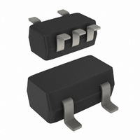
74AHCT1G79GW,165 NXP Semiconductors, 74AHCT1G79GW,165 Datasheet - Page 4

74AHCT1G79GW,165
Manufacturer Part Number
74AHCT1G79GW,165
Description
IC D F-F POS-EDGE TRIG SC88A-5
Manufacturer
NXP Semiconductors
Series
74AHCTr
Type
D-Typer
Datasheet
1.74AHCT1G79GW125.pdf
(12 pages)
Specifications of 74AHCT1G79GW,165
Function
Standard
Output Type
Non-Inverted
Number Of Elements
1
Number Of Bits Per Element
1
Frequency - Clock
90MHz
Delay Time - Propagation
5ns
Trigger Type
Positive Edge
Current - Output High, Low
8mA, 8mA
Voltage - Supply
4.5 V ~ 5.5 V
Operating Temperature
-40°C ~ 125°C
Mounting Type
Surface Mount
Package / Case
SC-70-5, SC-88A, SOT-323-5, SOT-353, 5-TSSOP
Logic Family
AHCT
Technology
CMOS
Number Of Bits
1
Number Of Elements
1
Clock-edge Trigger Type
Positive-Edge
Polarity
Non-Inverting
Operating Supply Voltage (typ)
5V
Package Type
TSSOP
Propagation Delay Time
11ns
Low Level Output Current
8mA
High Level Output Current
-8mA
Operating Supply Voltage (min)
4.5V
Operating Supply Voltage (max)
5.5V
Operating Temp Range
-40C to 125C
Operating Temperature Classification
Automotive
Mounting
Surface Mount
Pin Count
5
Lead Free Status / RoHS Status
Lead free / RoHS Compliant
Other names
74AHCT1G79GW-R
74AHCT1G79GW-R
935263007165
74AHCT1G79GW-R
935263007165
NXP Semiconductors
8. Limiting values
Table 5.
In accordance with the Absolute Maximum Rating System (IEC 60134). Voltages are referenced to GND (ground = 0 V).
[1]
[2]
9. Recommended operating conditions
Table 6.
Voltages are referenced to GND (ground = 0 V).
10. Static characteristics
Table 7.
Voltages are referenced to GND (ground = 0 V).
74AHC_AHCT1G79_5
Product data sheet
Symbol
V
V
I
I
I
I
I
T
P
Symbol Parameter
V
V
V
T
Symbol Parameter
For type 74AHC1G79
V
V
IK
OK
O
CC
GND
stg
amb
t/ V
CC
I
tot
CC
I
O
IH
IL
The input and output voltage ratings may be exceeded if the input and output current ratings are observed.
For both TSSOP5 and SC-74A packages: above 87.5 C the value of P
HIGH-level
input voltage
LOW-level
input voltage
supply voltage
input voltage
output voltage
ambient temperature
input transition rise
and fall rate
Limiting values
Recommended operating conditions
Static characteristics
Parameter
supply voltage
input voltage
input clamping current
output clamping current
output current
supply current
ground current
storage temperature
total power dissipation
Conditions
V
V
V
V
V
V
CC
CC
CC
CC
CC
CC
= 2.0 V
= 2.0 V
= 3.0 V
= 5.5 V
= 3.0 V
= 5.5 V
Conditions
V
V
CC
CC
= 3.3 V
= 5.0 V
Conditions
V
V
T
0.5 V < V
I
O
amb
< 0.5 V
< 0.5 V or V
= 40 C to +125 C
0.3 V
0.5 V
Rev. 05 — 2 July 2007
O
< V
3.85
Min
1.5
2.1
-
-
-
CC
74AHC1G79; 74AHCT1G79
O
> V
Min
+ 0.5 V
2.0
25 C
0
0
40
-
-
Typ
CC
-
-
-
-
-
-
tot
74AHC1G79
+ 0.5 V
derates linearly with 4.0 mW/K.
Max
1.65
Single D-type flip-flop; positive-edge trigger
Typ
+25
0.5
0.9
5.0
-
-
-
-
-
-
-
3.85
40 C to +85 C
Min
2.1
1.5
+125
Max
V
100
-
-
-
5.5
5.5
20
CC
[1]
[2]
Max
1.65
0.5
0.9
Min
4.5
-
-
-
Min
-
-
-
-
0
0
40
-
-
0.5
0.5
20
75
65
74AHCT1G79
40 C to +125 C Unit
3.85
Typ
+25
Min
5.0
1.5
2.1
-
-
-
-
-
-
-
Max
+7.0
+7.0
-
75
-
+150
250
© NXP B.V. 2007. All rights reserved.
20
25
+125
Max
V
5.5
5.5
20
Max
1.65
CC
-
0.5
0.9
-
-
-
Unit
V
V
mA
mA
mA
mA
mA
mW
C
Unit
V
V
V
ns/V
ns/V
C
4 of 12
V
V
V
V
V
V


