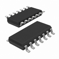
N74F74D,602 NXP Semiconductors, N74F74D,602 Datasheet - Page 4

N74F74D,602
Manufacturer Part Number
N74F74D,602
Description
IC FLIP FLOP DUAL D TYPE 14SOIC
Manufacturer
NXP Semiconductors
Series
74Fr
Type
D-Typer
Datasheet
1.N74F74N602.pdf
(8 pages)
Specifications of N74F74D,602
Function
Set(Preset) and Reset
Output Type
Differential
Number Of Elements
2
Number Of Bits Per Element
1
Frequency - Clock
125MHz
Trigger Type
Positive Edge
Current - Output High, Low
1mA, 20mA
Voltage - Supply
4.5 V ~ 5.5 V
Operating Temperature
-40°C ~ 85°C
Mounting Type
Surface Mount
Package / Case
14-SOIC (3.9mm Width), 14-SOL
Lead Free Status / RoHS Status
Lead free / RoHS Compliant
Delay Time - Propagation
-
Other names
568-1733-5
933739410602
N74F74D
933739410602
N74F74D
1 For conditions shown as MIN or MAX, use the appropriate value specified under recommended operating conditions for the applicable type.
2 All typical values are at V
3 Not more than one output should be shorted at a time. For testing I
4 Measure I
Philips Semiconductors
DC ELECTRICAL CHARACTERISTICS
(Over recommended operating free-air temperature range unless otherwise noted.)
NOTES:
AC ELECTRICAL CHARACTERISTICS
AC SETUP REQUIREMENTS
1996 Mar 12
SYMBOL
SYMBOL
SYMBOL
SYMBOL
V
V
V
V
V
I
I
I
I
I
I
f
t
t
t
t
t
t
t
t
t
t
t
t
I
IH
IL
OS
CC
max
PLH
PHL
PLH
PHL
su
su
h
h
w
w
w
rec
Dual D-type flip-flop
techniques are preferable in order to minimize internal heating and more accurately reflect operational values. Otherwise, prolonged shorting
of a high output may raise the chip temperature well above normal and thereby cause invalid readings in other parameter tests. In any
sequence of parameter tests, I
O
OH
O
OL
IK
(H)
(L)
(L)
(L)
(H)
(L)
(H)
Maximum clock frequency
High level output voltage
High-level output voltage
Low level output voltage
Low-level output voltage
Input clamp voltage
Input current at maximum input
voltage
High-level input current
Low-level input
current
Short-circuit output current
Supply current (total)
CC
Propagation delay
CPn to Qn or Qn
Propagation delay
SDn, RDn to Qn or Qn
Setup time, high or low
Dn to CPn
Hold time, high or low
Dn to CPn
CPn pulse width,
high or low
SDn, RDn pulse width,
low
Recovery time
SDn, RDn to CPn
with the clock input grounded and all outputs open, then with Q and Q outputs high in turn.
PARAMETER
PARAMETER
PARAMETER
PARAMETER
CC
= 5V, T
OS
SDn, RDn
4
Dn, CPn
tests should be performed last.
amb
3
CONDITION
CONDITION
Waveform 1
Waveform 1
Waveform 2
Waveform 1
Waveform 1
Waveform 1
Waveform 2
Waveform 3
= 25 C.
TEST
TEST
V
V
V
V
V
V
V
V
V
V
V
CC
CC
CC
CC
CC
CC
CC
CC
CC
CC
CC
= MIN V = MAX V
= MIN, V
= MIN V = MAX V
= MIN, V
= MIN, I
= MAX, V
= MAX, V
= MAX, V
= MAX, V
= MAX
= MAX
C
C
MIN
MIN
100
I
3.8
4.4
3.2
3.5
2.0
3.0
1.0
1.0
4.0
5.0
4.0
2.0
L
L
IL
IL
= I
I
I
I
I
= 50pF, R
= 50pF, R
= 7.0V
= 2.7V
= 0.5V
= 0.5V
= MAX, V
= MAX, V
T
T
V
V
IK
amb
amb
CC
CC
TEST CONDITIONS
TEST CONDITIONS
TYP
TYP
125
= +5.0V
5.3
6.2
4.6
7.0
= +5.0V
= +25 C
= +25 C
OS
4
L
L
IH
IH
, the use of high-speed test apparatus and/or sample-and-hold
= 500
= 500
= MIN
= MIN
= MIN
= MIN
MAX
MAX
6.8
8.0
6.1
9.0
I
I
I
I
C
C
O
OH
O
OL
T
T
V
V
L
L
amb
amb
CC
MIN
CC
MIN
1
1
100
= 50pF, R
3.8
4.4
3.2
3.5
= 50pF, R
2.0
3.0
1.0
1.0
4.0
5.0
4.0
2.0
= MAX
= MAX
= MAX
= MAX
= +5.0V
= +5.0V
= 0 C to +70 C
= 0 C to +70 C
LIMITS
LIMITS
L
L
10%V
10%V
5%V
5%V
= 500
MAX
= 500
MAX
10.5
7.8
9.2
7.1
10%
10%
CC
CC
CC
CC
T
T
C
C
amb
amb
MIN
-60
V
V
2.5
2.7
L
L
MIN
MIN
CC
CC
= 50pF, R
3.8
4.4
3.2
2.5
= 50pF, R
2.0
3.0
1.0
1.0
4.0
5.0
4.0
2.0
90
= –40 C to +85 C
= –40 C to +85 C
= +5.0V
= +5.0V
LIMITS
TYP
-0.73
0.30
0.30
11.5
3.4
2
L
L
Product specification
= 500
= 500
MAX
MAX
10.5
8.5
9.2
7.5
10%
10%
MAX
0.50
0.50
-150
-1.2
-0.6
-1.8
100
20
16
74F74
UNIT
UNIT
UNIT
UNIT
MHz
mA
mA
mA
mA
ns
ns
ns
ns
ns
ns
ns
V
V
V
V
V
A
A


