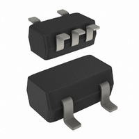
74LVC1G79GW,125 NXP Semiconductors, 74LVC1G79GW,125 Datasheet - Page 3

74LVC1G79GW,125
Manufacturer Part Number
74LVC1G79GW,125
Description
IC SGL D FF POS-EDG TRIG 5-TSSOP
Manufacturer
NXP Semiconductors
Series
74LVCr
Type
D-Typer
Datasheet
1.74LVC1G79GW125.pdf
(20 pages)
Specifications of 74LVC1G79GW,125
Output Type
Non-Inverted
Package / Case
SC-70-5, SC-88A, SOT-323-5, SOT-353, 5-TSSOP
Function
Standard
Number Of Elements
1
Number Of Bits Per Element
1
Frequency - Clock
500MHz
Delay Time - Propagation
1.7ns
Trigger Type
Positive Edge
Current - Output High, Low
32mA, 32mA
Voltage - Supply
1.65 V ~ 5.5 V
Operating Temperature
-40°C ~ 125°C
Mounting Type
Surface Mount
Number Of Circuits
1
Logic Family
LVC
Logic Type
D-Type Edge Triggered Flip-Flop
Polarity
Non-Inverting
Input Type
Single-Ended
Propagation Delay Time
2.2 ns at 3.3 V
High Level Output Current
- 32 mA
Low Level Output Current
32 mA
Supply Voltage (max)
5.5 V
Maximum Operating Temperature
+ 125 C
Mounting Style
SMD/SMT
Minimum Operating Temperature
- 40 C
Supply Voltage (min)
1.65 V
Technology
CMOS
Number Of Bits
1
Number Of Elements
1
Clock-edge Trigger Type
Positive-Edge
Operating Supply Voltage (typ)
1.8/2.5/3.3/5V
Package Type
SOT
Frequency (max)
200MHz
Operating Supply Voltage (min)
1.65V
Operating Supply Voltage (max)
5.5V
Operating Temp Range
-40C to 125C
Operating Temperature Classification
Automotive
Mounting
Surface Mount
Pin Count
5
Lead Free Status / RoHS Status
Lead free / RoHS Compliant
Lead Free Status / RoHS Status
Lead free / RoHS Compliant, Lead free / RoHS Compliant
Other names
568-4838-2
74LVC1G79GW,125
74LVC1G79GW-G
74LVC1G79GW-G
935268675125
74LVC1G79GW,125
74LVC1G79GW-G
74LVC1G79GW-G
935268675125
Available stocks
Company
Part Number
Manufacturer
Quantity
Price
Company:
Part Number:
74LVC1G79GW,125
Manufacturer:
NXP Semiconductors
Quantity:
7 050
NXP Semiconductors
6. Pinning information
Table 3.
74LVC1G79
Product data sheet
Symbol
D
CP
GND
Q
n.c.
V
Fig 3.
Fig 4.
CC
GND
CP
D
Pin configuration
SOT353-1 and SOT753
Logic diagram
Pin description
1
2
3
74LVC1G79
Pin
SOT353-1, SOT753
1
2
3
4
-
5
6.1 Pinning
6.2 Pin description
001aaf188
CP
D
5
4
V
Q
CC
TG
C
C
SOT886, SOT891, SOT1115 and SOT1202
1
2
3
4
5
6
All information provided in this document is subject to legal disclaimers.
Fig 5.
C
C
TG
Rev. 8 — 30 September 2010
C
C
GND
CP
Pin configuration SOT886
D
Transparent top view
74LVC1G79
1
2
3
TG
001aaf189
C
C
6
5
4
V
n.c.
Q
CC
Single D-type flip-flop; positive-edge trigger
TG
C
C
Fig 6.
Description
data input
data pulse input
ground (0 V)
data output
not connected
supply voltage
GND
CP
Pin configuration SOT891,
SOT1115 and SOT1202
mna442
D
Transparent top view
74LVC1G79
Q
74LVC1G79
1
2
3
© NXP B.V. 2010. All rights reserved.
001aaf410
6
5
4
V
n.c.
Q
CC
3 of 20


