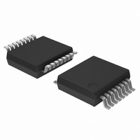
74HCT173DB,112 NXP Semiconductors, 74HCT173DB,112 Datasheet - Page 10

74HCT173DB,112
Manufacturer Part Number
74HCT173DB,112
Description
IC QUAD D F-F POS-EDGE 16-SSOP
Manufacturer
NXP Semiconductors
Series
74HCTr
Type
D-Type Busr
Datasheets
1.74HCT4046ADB112.pdf
(19 pages)
2.74HCT4046ADB112.pdf
(23 pages)
3.74HCT173DB112.pdf
(10 pages)
Specifications of 74HCT173DB,112
Output Type
Tri-State Non Inverted
Package / Case
16-SSOP
Function
Master Reset
Number Of Elements
4
Number Of Bits Per Element
1
Frequency - Clock
80MHz
Delay Time - Propagation
20ns
Trigger Type
Positive Edge
Voltage - Supply
4.5 V ~ 5.5 V
Operating Temperature
-40°C ~ 125°C
Mounting Type
Surface Mount
Number Of Circuits
1
Logic Family
HCT
Logic Type
D-Type Edge Triggered Flip-Flop
Polarity
Non-Inverting
Input Type
Single-Ended
Propagation Delay Time
17 ns
High Level Output Current
- 6 mA
Low Level Output Current
6 mA
Supply Voltage (max)
5.5 V
Maximum Operating Temperature
+ 125 C
Mounting Style
SMD/SMT
Minimum Operating Temperature
- 40 C
Supply Voltage (min)
4.5 V
Lead Free Status / RoHS Status
Lead free / RoHS Compliant
Current - Output High, Low
-
Lead Free Status / Rohs Status
Lead free / RoHS Compliant
Other names
568-2795-5
935189710112
935189710112
Philips Semiconductors
AC WAVEFORMS
December 1990
Quad D-type flip-flop; positive-edge trigger;
3-state
(1) HC : V
Fig.6
(1) HC : V
Fig.8
HCT: V
HCT: V
Waveforms showing the clock (CP) to
output (Q
pulse width, the output transition times and
the maximum clock pulse frequency.
Waveforms showing the 3-state enable and
disable times.
M
M
M
M
= 50%; V
= 50%; V
= 1.3 V; V
= 1.3 V; V
n
I
I
I
) propagation delays, the clock
I
= GND to V
= GND to V
= GND to 3 V.
= GND to 3 V.
CC
CC
.
.
10
PACKAGE OUTLINES
See
(1) HC : V
Fig.7
The shaded areas indicate when the input is permitted to
change for predictable output performance.
(1) HC : V
Fig.9 Waveforms showing the data set-up and hold
“74HC/HCT/HCU/HCMOS Logic Package Outlines”
HCT: V
HCT: V
times from input (En, D
Waveforms showing the master reset (MR)
pulse width, the master reset to output (Q
propagation delays and the master reset to
clock (CP) removal time.
M
M
M
M
= 50%; V
= 1.3 V; V
= 50%; V
= 1.3 V; V
I
I
I
I
= GND to V
= GND to V
= GND to 3 V.
= GND to 3 V.
CC
CC
.
.
n
74HC/HCT173
) to clock (CP).
Product specification
n
)
.


