74HCT574DB,112 NXP Semiconductors, 74HCT574DB,112 Datasheet - Page 4
74HCT574DB,112
Manufacturer Part Number
74HCT574DB,112
Description
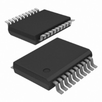
IC OCTAL D F-F POS-EDGE 20-SSOP
Manufacturer
NXP Semiconductors
Series
74HCTr
Type
D-Type Busr
Datasheets
1.74HCT4046ADB112.pdf
(19 pages)
2.74HCT4046ADB112.pdf
(23 pages)
3.74HC574D653.pdf
(19 pages)
Specifications of 74HCT574DB,112
Function
Standard
Output Type
Tri-State Non Inverted
Number Of Elements
1
Number Of Bits Per Element
8
Frequency - Clock
69MHz
Delay Time - Propagation
18ns
Trigger Type
Positive Edge
Voltage - Supply
4.5 V ~ 5.5 V
Operating Temperature
-40°C ~ 125°C
Mounting Type
Surface Mount
Package / Case
20-SSOP
Lead Free Status / RoHS Status
Lead free / RoHS Compliant
Current - Output High, Low
-
Other names
568-2890-5
935175110112
935175110112


NXP Semiconductors
Table 2.
6. Functional description
Table 3.
[1]
7. Limiting values
Table 4.
In accordance with the Absolute Maximum Rating System (IEC 60134). Voltages are referenced to GND (ground = 0 V).
[1]
[2]
74HC_HCT574
Product data sheet
Symbol
OE
D[0:7]
GND
CP
Q[0:7]
V
Operating mode
Load and read register
Load register and disable output
Symbol
V
I
I
I
I
I
T
P
IK
OK
O
CC
GND
stg
CC
CC
tot
H = HIGH voltage level;
h = HIGH voltage level one setup time prior to the HIGH-to-LOW CP transition;
L = LOW voltage level;
l = LOW voltage level one setup time prior to the HIGH-to-LOW CP transition;
Z = high-impedance OFF-state;
= LOW-to-HIGH clock transition.
For DIP20 package: P
For SO20: P
For SSOP20 and TSSOP20 packages: P
Pin description
Function table
Limiting values
Pin
1
2, 3, 4, 5, 6, 7, 8, 9
10
11
19, 18, 17, 16, 15, 14, 13, 12 3-state flip-flop output
20
Parameter
supply voltage
input clamping current
output clamping current
output current
supply current
ground current
storage temperature
total power dissipation
tot
derates linearly with 8 mW/K above 70 C.
5.2 Pin description
tot
derates linearly with 12 mW/K above 70 C.
[1]
tot
All information provided in this document is subject to legal disclaimers.
Conditions
V
V
V
derates linearly with 5.5 mW/K above 60 C.
Description
3-state output enable input (active LOW)
data input
ground (0 V)
clock input (LOW-to-HIGH, edge triggered)
supply voltage
I
O
O
Input
OE
L
L
H
H
DIP20 package
SO20, SSOP20 and TSSOP20 packages
< 0.5 V or V
< 0.5 V or V
= 0.5 V to (V
Rev. 3 — 15 December 2010
I
O
CP
> V
CC
> V
CC
+ 0.5 V)
Octal D-type flip-flop; positive edge-trigger; 3-state
CC
+ 0.5 V
+ 0.5 V
Dn
l
h
l
h
74HC574; 74HCT574
Internal
flip-flop
L
H
L
H
[1]
[2]
Min
0.5
-
-
-
-
-
65
-
-
© NXP B.V. 2010. All rights reserved.
Max
+7
20
20
35
+70
70
+150
750
500
Output
Qn
L
H
Z
Z
Unit
V
mA
mA
mA
mA
mA
C
mW
mW
4 of 19
Related parts for 74HCT574DB,112
Image
Part Number
Description
Manufacturer
Datasheet
Request
R

Part Number:
Description:
IC FLIP FLOP OCTAL D 3ST 20SOIC
Manufacturer:
NXP Semiconductors
Datasheet:

Part Number:
Description:
Flip Flop D-Type Bus Interface Pos-Edge 3-ST 1-Element 20-Pin SO Bulk
Manufacturer:
NXP Semiconductors
Datasheet:
Part Number:
Description:
IC FLIP FLOP OCTAL D 3ST 20SOIC
Manufacturer:
NXP Semiconductors
Datasheet:
Part Number:
Description:
NXP Semiconductors designed the LPC2420/2460 microcontroller around a 16-bit/32-bitARM7TDMI-S CPU core with real-time debug interfaces that include both JTAG andembedded trace
Manufacturer:
NXP Semiconductors
Datasheet:

Part Number:
Description:
NXP Semiconductors designed the LPC2458 microcontroller around a 16-bit/32-bitARM7TDMI-S CPU core with real-time debug interfaces that include both JTAG andembedded trace
Manufacturer:
NXP Semiconductors
Datasheet:
Part Number:
Description:
NXP Semiconductors designed the LPC2468 microcontroller around a 16-bit/32-bitARM7TDMI-S CPU core with real-time debug interfaces that include both JTAG andembedded trace
Manufacturer:
NXP Semiconductors
Datasheet:
Part Number:
Description:
NXP Semiconductors designed the LPC2470 microcontroller, powered by theARM7TDMI-S core, to be a highly integrated microcontroller for a wide range ofapplications that require advanced communications and high quality graphic displays
Manufacturer:
NXP Semiconductors
Datasheet:
Part Number:
Description:
NXP Semiconductors designed the LPC2478 microcontroller, powered by theARM7TDMI-S core, to be a highly integrated microcontroller for a wide range ofapplications that require advanced communications and high quality graphic displays
Manufacturer:
NXP Semiconductors
Datasheet:
Part Number:
Description:
The Philips Semiconductors XA (eXtended Architecture) family of 16-bit single-chip microcontrollers is powerful enough to easily handle the requirements of high performance embedded applications, yet inexpensive enough to compete in the market for hi
Manufacturer:
NXP Semiconductors
Datasheet:
Part Number:
Description:
The XA-S3 device is a member of Philips Semiconductors? XA(eXtended Architecture) family of high performance 16-bitsingle-chip microcontrollers
Manufacturer:
NXP Semiconductors
Datasheet:

Part Number:
Description:
The NXP BlueStreak LH75401/LH75411 family consists of two low-cost 16/32-bit System-on-Chip (SoC) devices
Manufacturer:
NXP Semiconductors
Datasheet:
Part Number:
Description:
The NXP LPC3130/3131 combine an 180 MHz ARM926EJ-S CPU core, high-speed USB2
Manufacturer:
NXP Semiconductors
Datasheet:
Part Number:
Description:
The NXP LPC3141 combine a 270 MHz ARM926EJ-S CPU core, High-speed USB 2
Manufacturer:
NXP Semiconductors
Part Number:
Description:
The NXP LPC3143 combine a 270 MHz ARM926EJ-S CPU core, High-speed USB 2
Manufacturer:
NXP Semiconductors